Engineering High-Performance CIGS Solar Cells: Structural Design and Process Development

Engineering High-Performance CIGS Solar Cells: Structural Design and Process Development

Received: 05 March 2026 Revised: 31 March 2026 Accepted: 08 April 2026 Published: 27 April 2026

© 2026 The authors. This is an open access article under the Creative Commons Attribution 4.0 International License (https://creativecommons.org/licenses/by/4.0/).
Graphical Abstract
1. Introduction
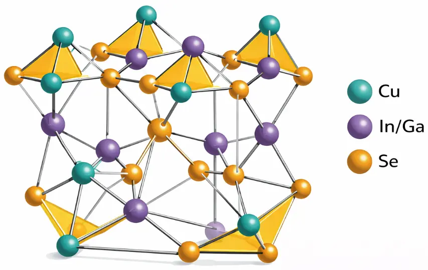
The pursuit of sustainable energy resources has led to the exponential development of solar cell technologies, with a focus on achieving high power conversion efficiency (PCE) [1]. Within this landscape, copper indium gallium diselenide (CIGS) is highlighted as being one of the most promising semiconductors owing to low price, high absorption coefficient, tunable band gap, low radiation damage, and long-term stability [2,3]. CIGS is a p-type quaternary compound semiconductor and a solid-solution material belonging to the I–III–VI₂ family. It exhibits a chalcopyrite crystal framework with tetrahedrally coordinated atomic bonding, as schematically illustrated in Figure 1 [4]. The performance of CIGS solar cells is strongly influenced by Ga and In composition, which enables bandgap tuning and efficiency enhancement [5,6]. In particular, gallium content plays a crucial role in improving open-circuit voltage, while numerical modeling approaches provide further insight into device optimization [7,8,9]. The material is characterized by a direct bandgap with a high absorption coefficient of $${10}^{5} \,{\mathrm{c}\mathrm{m}}^{-1}$$ [10], which allows the absorber layer to absorb a significant portion of solar radiation with only 2–4 µm thick film [11]. This thickness is roughly 100 times less than the thickness of a c-Si wafer-based Pv cell, which is in the range of 150–200 µm [12].
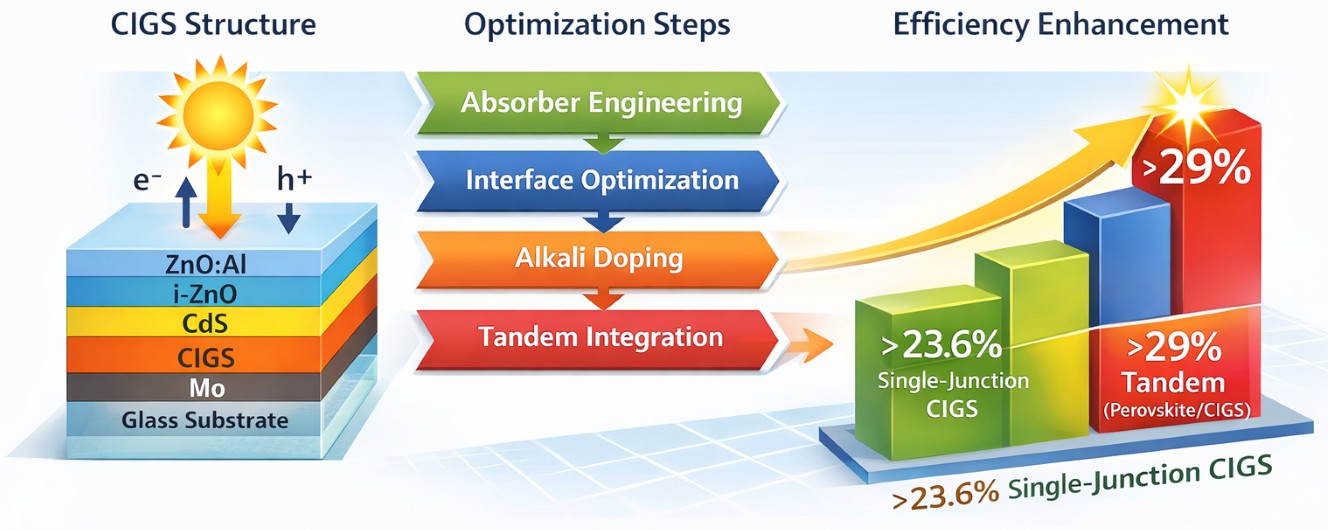
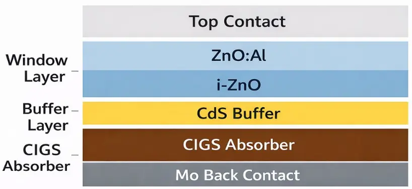
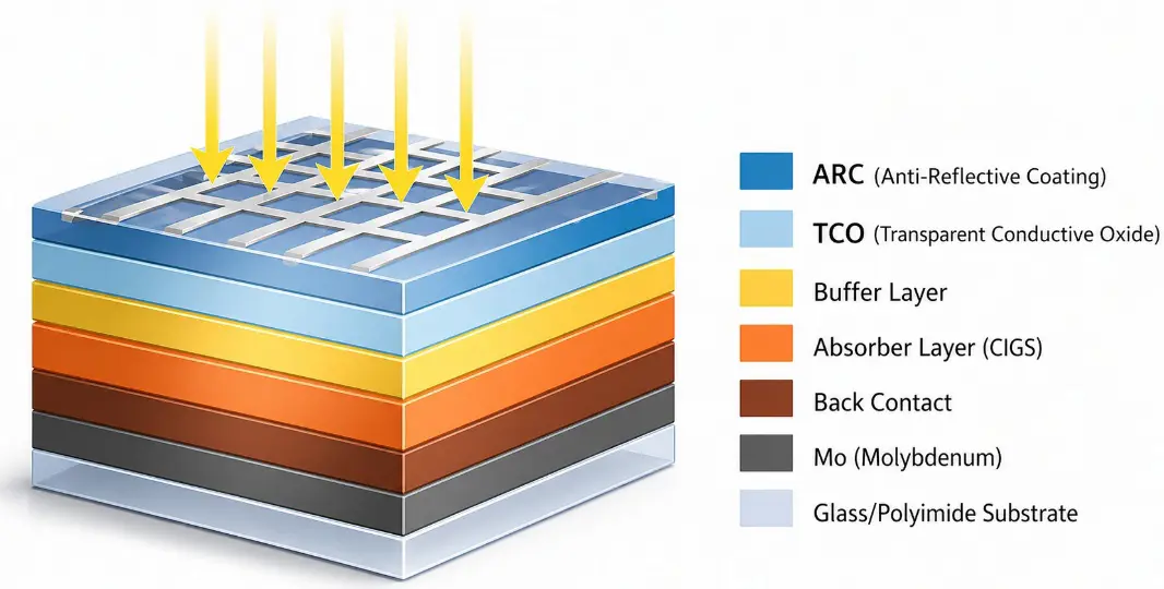
The architecture of a state-of-the-art high-performance device is critical for optimizing optoelectronic properties. A typical CIGS-based TFSC is a heterojunction solar cell composed of a conventional multilayer stack consisting of soda-lime glass (SLG), Mo back contact, CIGS absorber, buffer layer, window layer, and top metal contact, as illustrated in Figure 2 [13]. In the substrate configuration, incident light enters the cell through the transparent conducting oxide (TCO) front side, while the back contact is deposited on the supporting substrate, as illustrated in Figure 3 [14]. To reach the laboratory record efficiency of 23.6% achieved in early 2023 [10], structural engineering of the interfaces is paramount. This approach relates to the deposition of n-type buffer layers on the CIGS layer, elemental inter-diffusion at CIGS/buffer layer interfaces, presence of ordered vacancy defects, compositional deviation, and the formation of a concomitant $$p-n$$ junction [15,16,17,18].
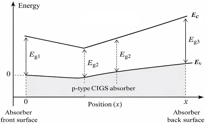
Specifically, the implementation of a double profiling structure, known as a notch structure, utilizes higher $$Ga$$ content towards the front and the back of the CIGS absorber layer and low $$Ga$$ content in between them Figure 4 [14]. As illustrated in Figure 5, front-side grading enhances the open-circuit voltage ($${V}_{oc}$$), whereas back-side grading improves the short-circuit current ($${I}_{sc}$$) [14].
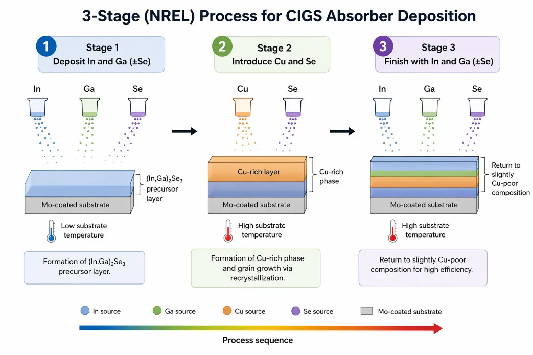
Process development remains a primary focus for commercializing high-performance cells, prioritizing stoichiometry, efficiency, high-throughput, and reproducibility [14]. For the preparation of the CIGS film, vacuum-based techniques such as co-evaporation and sputtering are more preferable due to the formation of smooth and pinholes-free morphology with controllable thickness over a large area [10]. The three-stage process (NREL process), Figure 6, which involves depositing In and Ga in the first stage, Cu in the second stage, and finishing with In and Ga to provide a graded profile, has currently given the highest efficiency [11]. Furthermore, doping with alkali metals, such as $$Li$$, $$Na$$, $$K$$, $$Rb$$, and $$Cs$$, can effectively modify the bandgap and optimize the PCE of the absorber layer [1]. In addition to terrestrial applications, these high-performance engineered cells are suitable candidates for space applications due to their high radiation tolerance [19].
The corresponding energy band diagram of the CIGS solar cell is illustrated in Figure 4. The diagram illustrates band alignment, carrier transport mechanisms, and heterojunction behavior within the device.
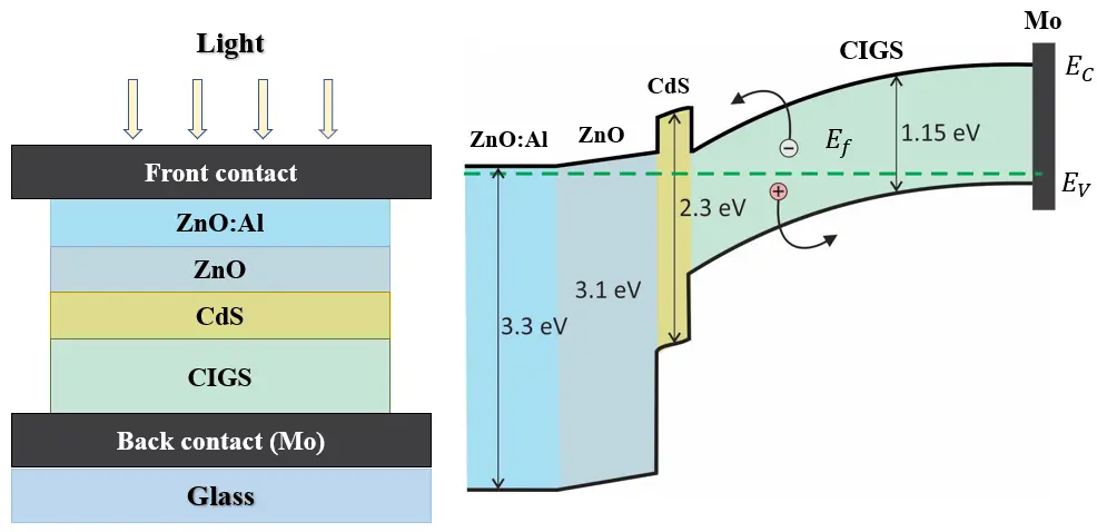
Figure 4. Schematic structure and energy band diagram of the CIGS solar cell showing the conduction band (Ec), valence band (Ev), and Fermi level (Ef) across ZnO:Al/ZnO/CdS/CIGS/Mo layers, illustrating band alignment, heterojunction formation, and charge transport mechanisms.
The energy band diagram provides a clear physical interpretation of band alignment and carrier transport across the device. The heterojunction formed at the CdS/CIGS interface facilitates efficient separation of photogenerated carriers, while band bending enhances carrier collection and minimizes recombination losses. The band alignment between different layers plays a crucial role in determining the overall device performance.
Furthermore, the continuous development of thin-film photovoltaic technologies requires a deeper understanding of material properties and device optimization strategies.
CIGS solar cells represent a high-efficiency thin-film photovoltaic technology, whose optoelectronic properties can be effectively tuned through compositional engineering [6,20,21,22]. Advanced strategies such as absorber thickness optimization and deposition techniques, including magnetron sputtering, have been shown to significantly enhance device performance [5,23,24,25]. Furthermore, the incorporation of novel buffer layers and back surface field (BSF) structures plays a crucial role in improving charge carrier collection and overall energy conversion efficiency [23,26].
This report details the structural design paradigms and fabrication advancements essential for the next generation of power-efficient CIGS solar cells.
2. Integrated Optimization of CIGS: Synthesis, Doping, and Advanced Device Architectures
Advanced Bandgap Engineering via Double Grading. To mitigate the efficiency constraints inherent in single-junction devices, a primary structural optimization involves the implementation of a double profiling structure of the absorber composition, known as a notch structure Figure 4. This architecture utilizes a higher Ga content towards the front and the back of the CIGS absorber layer and low Ga content in between them Figure 5 [14]. The resulting “V” type band structure boosts light absorption, accelerates charge transport, reduces recombination, and increases $${V}_{oc}$$ [4]. Specifically, front side grading improves $${V}_{oc}$$, while back grading improves $${J}_{sc}$$ Figure 5 [14].
The back surface field (BSF) created by this Ga gradient reflects electrons towards the p–n junction to be finally collected by the n-type electrode, thereby reducing minority carrier recombination at the rear CIGS/Mo interface [14]. This precise modulation of the Ga/In ratio through the absorber depth creates a graded bandgap composition (typically 1.04 eV to 1.7 eV) that provides a better match to the solar spectrum [4].
Interface Engineering and Surface Passivation. A critical solution for reducing open-circuit voltage deficits is the engineering of the absorber/buffer interface. Recombination at the heterogeneous $$CI\left(G\right)S/CdS$$ interface is effectively reduced by the formation of an ordered vacancy compound (OVC or ordered defect compound, ODC), which acts as a buried pn junction [12]. Furthermore, doping with alkali metals—$$Li$$, $$Na$$, $$K$$, $$Rb$$, and $$Cs$$—is proposed to modify the bandgap and optimize the PCE [1].
Heavy alkali metals like $$Rb$$ and $$Cs$$ contribute to phase formation with $$Se$$ and In at the surface, which improves band alignment at the interface and enhances electrical properties [1]. The implementation of alkali doping via post-deposition treatment (PDT) is a primary strategy to enhance the p–n junction interface [1]. For instance, $$K$$ doping facilitates the diffusion of $$Cd$$ into the $$Cu$$-depleted surface, improving the quality of the $$CIGS/CdS$$ interface [28].
Buffer Layer and Window Layer Optimization. To address the parasitic absorption of high-energy photons caused by conventional $$CdS$$, structural optimization favors the use of wide-bandgap, $$Cd$$-free buffer layers. Atomic Layer Deposition (ALD) is identified as a superior technique for producing uniform and conformal films like $$Zn\left(O, S\right)$$, $$ZnMgO$$, and $$ZnSnO$$ [13]. These materials provide a higher bandgap than $$CdS$$, which leads to lower absorption losses [11].
Proper formation of the conduction band offset ($$CBO$$) is essential; a moderate spike (positive $$CBO$$) within the range of 0–0.4 eV at the CIGS/buffer interface is favorable as it does not harm current collection [29,30]. Conversely, a cliff (negative CBO) decreases the barrier at the interface and increases recombination, leading to voltage losses [31]. Window layer optimization involves the use of $$i-ZnO$$ to act as a blocking layer for shunt paths between the front contact and absorber layer [11].
Technological Pathways for Implementation. The most effective fabrication pathway to achieve these optimized structures is the vacuum-based three-stage co-evaporation process (NREL process) Figure 6 [14]. This sequence involves [27]:
-
-
Stage 1: Depositing $$In$$ and $$Ga$$ at a lower substrate temperature to form an $${\left(In,Ga\right)}_{2}{Se}_{3}$$ precursor layer.
-
-
Stage 2: Introducing $$Cu$$ and $$Se$$ at a higher temperature to form a $$Cu$$-rich phase, which promotes the growth of large grain sizes through recrystallization.
-
-
Stage 3: Finishing with $$In$$ and $$Ga$$ evaporation to return to a slightly $$Cu$$-poor composition, which is necessary for high efficiency.
Alternatively, sequential processing involving sputtering followed by sulfurization-after-selenization (SAS) provides the highest device performance for large-area production [10]. For flexible applications, low-temperature co-evaporation on polyimide (PI) substrates is essential, often requiring ex situ alkali-PDT to achieve efficiencies exceeding 20% [32].
3. Beyond Single-Junction Limits: Tandem Architectures and Optical Management in CIGS Photovoltaics
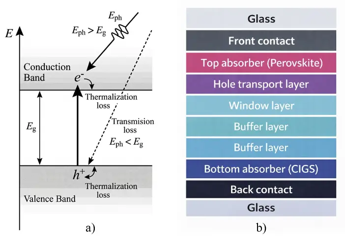
Theoretical Imperative for Tandem Architectures. Single-junction CIGS photovoltaics, while demonstrating high efficiency, are fundamentally capped by the 33.7% Shockley–Queisser limit [3,32]. This thermodynamic constraint mainly originates from two dominant losses: the transmission of sub-bandgap photons and the thermal relaxation of photogenerated hot carriers, as illustrated in Figure 7a [10]. Reducing the bandgap increases light absorption and enhances short-circuit current density ($${J}_{sc}$$), but the open-circuit voltage ($${V}_{oc}$$) remains constrained by carrier thermalization losses [10]. Tandem configurations overcome this limitation by combining a wide-bandgap top subcell with a narrow-bandgap bottom subcell, thereby broadening solar spectrum utilization, as shown in Figure 7b. This approach provides a pathway to exceed the SQ limit [4]. Theoretical calculations indicate that a two-junction device could boost efficiency up to 46% [10].
Structural Paradigms: Two-Terminal (2T) vs. Four-Terminal (4T) Systems. Realizing these efficiencies requires precise structural integration. Perovskite/CIGS tandem cells hold great promise (Table 1) because the bandgaps of both absorbers can be easily tailored for current matching conditions [19].
-
-
Two-Terminal (2T) Monolithic Tandems: These devices are processed on a single substrate and connected in series via an interconnecting layer [10]. This architecture is industry-preferred as it requires fewer deposition steps, minimizes optical and series resistance losses, and offers significant cost savings in manufacturing [10]. However, the device short-circuit current ($${J}_{total}$$) is limited by the subcell with the lower current, necessitating meticulous current matching [33].
-
-
Four-Terminal (4T) Mechanical Stacks: In this configuration, subcells are processed separately on different substrates and stacked, as shown in Figure 7b [10]. This avoids current-matching constraints and allows for wider selections of bandgap combinations [10]. Despite this flexibility, 4T systems incur higher costs due to additional cabling and inverters, as well as optical losses from the airgap between subcells [10].
Table 1. Comparison of perovskite-based tandem solar cell configurations.
|
Subcell Pairing |
Bandgap Range (eV) |
Development Status |
Technology Readiness Level (TRL) |
|---|---|---|---|
|
Perovskite/c-Si |
1.7–1.8/1.1 |
Approaching 30% efficiency |
6–7 |
|
Perovskite/CIGS |
1.6–2.3/1.04–1.68 |
High flexibility, space potential |
6–7 |
|
Perovskite/Perovskite |
1.7–1.9/1.2 |
High-cost potential, stability issues |
Early stage (Nascent) |
Advanced Optical Management and Bandgap Engineering. Optical management is considered a crucial factor for boosting the tandem efficiency [10]. To achieve maximum performance, the subcell bandgaps must be optimized for spectral splitting.
-
-
Bandgap Tunability: CIGS can achieve a tunable bandgap between 0.9 and 1.0 eV, which is favorable for the realization of the highest theoretical efficiency, whereas silicon ($$c-Si$$) has a fixed bandgap of 1.1 eV. This tunability enables reduced parasitic light absorption and suppressed photocurrent loss [4].
-
-
Anti-Reflective Coatings (ARC): Reflection losses originate from multiple interfaces in the device stack. Depositing a 150 nm thick $$Mg{F}_{2}$$ anti-reflective coating on the rear sides of perovskite top subcells can improve NIR transmittance by up to 8.6% [10].
-
-
Interconnecting Layers: The transparent conductive oxide (TCO) used as an interconnecting layer must be optimized. Reducing the AZO layer thickness to approximately 35 nm can significantly reduce series resistance while increasing light transmittance to the bottom subcell [10].
Performance Comparison. The following Table 2 highlights the efficiency benchmarks for single-junction and tandem CIGS-based architectures.
Table 2. Comparison of Device Efficiencies across Architectures.
|
Technology |
Architecture |
Champion Cell PCE (%) |
Theoretical Limit (%) |
Key Advantage |
|---|---|---|---|---|
|
CIGS (Single) |
Substrate (Single-junction) |
23.6% [10] |
~33.7% [32] |
Mature, high stability, flexible [10] |
|
Perovskite/CIGS (2T) |
Monolithic (Double-junction) |
24.2% [4] |
~46% [10] |
Simplified integration, lower parasitic loss [10] |
|
Perovskite/CIGS (4T) |
Mechanical Stack |
29.0% [10] |
~46% [10] |
No current matching required, spectral tolerance [10] |
|
All-CIGS (Simulated) |
2T Tandem (WS2 Buffer) |
41.10% [33] |
>40% [33] |
Ultra-high performance, $$Cd$$-free [33] |
4. Conclusions
The evolution of CIGS photovoltaics from single-junction films to sophisticated tandem systems represents a significant shift toward the next generation of power-efficient energy resources. Research indicates that the synergy between bandgap tunability (1.04 to 1.7 eV) and interfacial engineering–specifically through Cd-free buffer layers and alkali doping—has already pushed laboratory efficiencies to 23.6%. Transitioning to tandem structures further unlocks the theoretical potential to 46%, with current perovskite/CIGS mechanical stacks already reaching 29.0%. While 2T monolithic designs offer the most streamlined industrial pathway, success remains contingent on meticulous current matching and the optimization of transparent interconnecting layers. Ultimately, the continued refinement of co-evaporation and sequential processing ensures that CIGS remains a cornerstone of flexible, stable, and ultra-high-efficiency solar technology.
The findings of this study highlight the critical role of compositional engineering and interface optimization in achieving high-performance CIGS solar cells. Furthermore, these results provide valuable guidance for the development and large-scale implementation of next-generation photovoltaic systems in both industrial and sustainable energy applications.
Statement of the Use of Generative AI and AI-Assisted Technologies in the Writing Process
During the preparation of this manuscript, the authors used ChatGPT (OpenAI) to assist with language editing and refinement. After using this tool, the authors carefully reviewed and edited the content and take full responsibility for the content of the published article.
Author Contributions
Conceptualization, A.K.; Methodology, D.I.; Software, D.I.; Validation, D.I. and A.K.; Formal Analysis, D.I.; Investigation, D.I.; Resources, A.K.; Data Curation, D.I.; Writing—Original Draft Preparation, D.I.; Writing—Review & Editing, D.I. and A.K.; Visualization, D.I.; Supervision, A.K.; Project Administration, A.K.
Ethics Statement
Not applicable.
Informed Consent Statement
Not applicable.
Data Availability Statement
No new data were created or analyzed in this study. Data sharing is not applicable.
Funding
This research received no external funding.
Declaration of Competing Interest
The authors declare that they have no known competing financial interests or personal relationships that could have appeared to influence the work reported in this paper.
References
-
Amrillah T, Rizki IN, Alviani VN. From binary to quaternary copper chalcogenide compounds in solar cells technology: Recent progress and perspectives. Sol. Energy 2025, 299, 113784. DOI:10.1016/j.solener.2025.113784 [Google Scholar]
-
Lee S, Lee ES, Kim TY, Cho JS, Eo YJ, Yun JH, et al. Effect of annealing treatment on CdS/CIGS thin film solar cells depending on different CdS deposition temperatures. Sol. Energy Mater. Sol. Cells 2015, 141, 299–308. DOI:10.1016/j.solmat.2015.05.052 [Google Scholar]
-
Komilov A. Gallium content-dependent efficiency limits of CIGS solar cells at AM1.5G solar irradiance. J. Photonics Energy 2021, 11, 035501. DOI:10.1117/1.jpe.11.035501 [Google Scholar]
-
Chi W, Banerjee SK. Comparison and integration of CuInGaSe and perovskite solar cells. J. Energy Chem. 2023, 78, 463–475. DOI:10.1016/j.jechem.2022.12.039 [Google Scholar]
-
Salhi B. The Photovoltaic Cell Based on CIGS: Principles and Technologies. Materials 2022, 15, 1908. DOI:10.3390/ma15051908 [Google Scholar]
-
Sivasankar SM, Amorim CDO, Cunha AFD. Progress in Thin-Film Photovoltaics: A Review of Key Strategies to Enhance the Efficiency of CIGS, CdTe, and CZTSSe Solar Cells. J. Compos. Sci. 2025, 9, 143. DOI:10.3390/jcs9030143 [Google Scholar]
-
Lv X, Zheng Z, Zhao M, Wang H, Zhuang D. Investigation on Preparation and Performance of High Ga CIGS Absorbers and Their Solar Cells. Materials 2023, 16, 2806. DOI:10.3390/ma16072806 [Google Scholar]
-
Jafari SMH, Orouji AA, Abbasi A. Numerical investigation of ultrathin CIGS solar cells featuring SiO2/GaAs double rear passivation. Sci. Rep. 2026, 16, 4549. DOI:10.1038/s41598-025-34707-8 [Google Scholar]
-
Wu Z, Tao S, Jia M, Han J, Zhou J, Baranova M, et al. Bandgap Engineering of CIGS: Active Control of Composition Gradient. Energies 2025, 18, 6089. DOI:10.3390/en18236089 [Google Scholar]
-
Mohamad Noh MF, Arzaee NA, Fat CC, Sieh Kiong T, Mat Teridi MA, Mahmood Zuhdi AW. Perovskite/CIGS tandem solar cells: Progressive advances from technical perspectives. Mater. Today Energy 2024, 39, 101473. DOI:10.1016/j.mtener.2023.101473 [Google Scholar]
-
Kumar V, Prasad R, Chaure NB, Singh UP. Advancement in Copper Indium Gallium Diselenide (CIGS)-Based Thin-Film Solar Cells. In Recent Advances in Thin Film Photovoltaics; Springer: Singapore, 2022. DOI:10.1007/978-981-19-3724-8_2 [Google Scholar]
-
Petrova-Koch V, Hezel R, Goetzberger A. High-Efficient Low Cost Photovoltaics; Saule Chapter; Springer: Cham, Switzerland, 2009. DOI:10.1007/978-3-030-22864-4 [Google Scholar]
-
Sinha S, Nandi DK, Pawar PS, Kim SH, Heo J. A review on atomic layer deposited buffer layers for Cu(In,Ga)Se2 (CIGS) thin film solar cells: Past, present, and future. Sol. Energy 2020, 209, 515–537. DOI:10.1016/j.solener.2020.09.022 [Google Scholar]
-
Ramanujam J, Singh UP. Copper indium gallium selenide based solar cells—A review. Energy Environ. Sci. 2017, 10, 1306–1319. DOI:10.1039/c7ee00826k [Google Scholar]
-
Han A, Zhang Y, Song W, Li B, Liu W, Sun Y. Structure, morphology and properties of thinned Cu(In,Ga)Se2 films and solar cells. Semicond. Sci. Technol. 2012, 27, 035022. DOI:10.1088/0268-1242/27/3/035022 [Google Scholar]
-
Ishizuka S, Yamada A, Fons P, Niki S. Texture and morphology variations in (In,Ga)2Se3 and Cu(In,Ga)Se2 thin films grown with various Se source conditions. Prog. Photovolt. Res. Appl. 2013, 21, 544–553. DOI:10.1002/pip.1227 [Google Scholar]
-
Su CY, Ho WH, Lin HC, Nieh CY, Liang SC. The effects of the morphology on the CIGS thin films prepared by CuInGa single precursor. Sol. Energy Mater. Sol. Cells 2011, 95, 261–263. DOI:10.1016/j.solmat.2010.04.072 [Google Scholar]
-
Komilov AG, Nasrullaev YZ. Influence of the Environment on the Parameters of CIGS-Based Photovoltaic and Photovoltaic-Thermal Converters Used in Real Conditions. Appl. Sol. Energy 2021, 57, 8–12. DOI:10.3103/S0003701X21010047 [Google Scholar]
-
Lin L, Ravindra NM. Temperature dependence of CIGS and perovskite solar cell performance: An overview. SN Appl. Sci. 2020, 2, 1361. DOI:10.1007/s42452-020-3169-2 [Google Scholar]
-
Alarifi IM. Advanced selection materials in solar cell efficiency and their properties—A comprehensive review. Mater. Today Proc. 2021, 81, 403–414. DOI:10.1016/j.matpr.2021.03.427 [Google Scholar]
-
Lin L, Ravindra NM. CIGS and perovskite solar cells—An overview. Emerg. Mater. Res. 2020, 9, 812–824. DOI:10.1680/jemmr.20.00124 [Google Scholar]
-
Li H, Qu F, Luo H, Niu X, Chen J, Zhang Y, et al. Engineering CIGS grains qualities to achieve high efficiency in ultrathin Cu(InxGa1−x)Se2 solar cells with a single-gradient band gap profile. Results Phys. 2019, 12, 704–711. DOI:10.1016/j.rinp.2018.12.043 [Google Scholar]
-
Machkih K, Oubaki R, Makha M. A Review of CIGS Thin Film Semiconductor Deposition via Sputtering and Thermal Evaporation for Solar Cell Applications. Coatings 2024, 14, 1088. DOI:10.3390/coatings14091088 [Google Scholar]
-
Movla H. Optimization of the CIGS based thin film solar cells: Numerical simulation and analysis. Optik 2014, 125, 67–70. DOI:10.1016/j.ijleo.2013.06.034 [Google Scholar]
-
Sun X, Silverman T, Garris R, Deline C, Alam MA. An Illumination-and Temperature-Dependent Analytical Model for Copper Indium Gallium Diselenide (CIGS) Solar Cells. IEEE J. Photovolt. 2016, 6, 1298–1307. DOI:10.1109/JPHOTOV.2016.2583790 [Google Scholar]
-
Rahman MF, Hasan MK, Chowdhury M, Islam MR, Rahman MH, Rahman MA, et al. A qualitative Design and optimization of CIGS-based Solar Cells with Sn2S3 Back Surface Field: A plan for achieving 21.83% efficiency. Heliyon 2023, 9, e22866. DOI:10.1016/j.heliyon.2023.e22866 [Google Scholar]
-
Chirilǎ A, Reinhard P, Pianezzi F, Bloesch P, Uhl AR, Fella C, et al. Potassium-induced surface modification of Cu(In,Ga)Se2 thin films for high-efficiency solar cells. Nat. Mater. 2013, 12, 1107–1111. DOI:10.1038/nmat3789 [Google Scholar]
-
Minemoto T, Matsui T, Takakura H, Hamakawa Y, Negami T, Hashimoto Y, et al. Theoretical analysis of the effect of conduction band offset of window/CIS layers on performance of CIS solar cells using device simulation. Sol. Energy Mater. Sol. Cells 2001, 67, 83–88. DOI:10.1016/S0927-0248(00)00266-X [Google Scholar]
-
Siebentritt S. Alternative buffers for chalcopyrite solar cells. Sol. Energy 2004, 77, 767–775. DOI:10.1016/j.solener.2004.06.018 [Google Scholar]
-
Platzer-Björkman C, Lu J, Kessler J, Stolt L. Interface study of CuInSe2/ZnO and Cu(In,Ga)Se2/ZnO devices using ALD ZnO buffer layers. Thin Solid Films 2003, 431–432, 321–325. DOI:10.1016/S0040-6090(03)00229-3 [Google Scholar]
-
Stephan C. Structural Trends in off Stoichiometric Chalcopyrite Type Compound Semiconductors. Ph.D. Thesis, Freien Universität Berlin, Berlin, Germany, 2011. DOI:10.5442/d0011 [Google Scholar]
-
Intal D, Ebong AU. Thin-film solar photovoltaics: Trends and future directions. Renew. Sustain. Energy Rev. 2026, 226, 116464. DOI:10.1016/j.rser.2025.116464 [Google Scholar]
-
Mohammadi R, Hayati M, Shama F. High-efficiency monolithic CIGS/CIGS tandem solar cell with WS2 buffer layers. Micro Nanostruct. 2026, 213, 208589. DOI:10.1016/j.micrna.2026.208589 [Google Scholar]