Recent Progress in Photonic Design and Charge Transport Optimization for Organic Solar Cells

Recent Progress in Photonic Design and Charge Transport Optimization for Organic Solar Cells
Received: 08 November 2025 Revised: 15 December 2025 Accepted: 29 January 2026 Published: 13 March 2026

© 2026 The authors. This is an open access article under the Creative Commons Attribution 4.0 International License (https://creativecommons.org/licenses/by/4.0/).
1. Introduction
With global energy demand continuing to rise, the rapid transition to sustainable and renewable energy sources has become increasingly critical. Single-junction organic solar cells (OSCs) have emerged as a promising photovoltaic technology due to their mechanical flexibility, low weight, and compatibility with low-cost, large-area solution processing. Beyond these inherent advantages, OSCs have matured significantly through continuous advances in materials chemistry, device architecture, and interfacial engineering. In particular, the transition from fullerene-based acceptors to non-fullerene acceptors has enabled broader spectral absorption, reduced energy losses, and improved morphological stability, leading to substantial gains in power conversion efficiency. Parallel progress in optical management and device design has further enhanced light utilization and charge extraction in ultrathin active layers. Collectively, these developments position single-junction OSCs as competitive alternatives to conventional silicon photovoltaics for flexible and emerging applications such as wearable electronics, building-integrated photovoltaics, and portable power generation [1,2,3,4,5]. Additionally, solution-based fabrication methods, such as roll-to-roll printing, enable scalable, cost-effective production, supporting the development and commercial use of these devices. One major advantage of single-junction OSCs is their adjustable optoelectronic properties. Researchers can design the small molecular structure of organic semiconductors to maximize light absorption across different wavelengths, which can significantly improve power conversion efficiency (PCE). In organic solar cells, the PCE measures the ratio of the maximum electrical output power to the incident solar power under standard lighting conditions. It is calculated by multiplying the short-circuit current density (Jsc), open-circuit voltage (Voc), and fill factor (FF) using the formula:
|
```latex\mathrm{P}\mathrm{C}\mathrm{E}=\mathrm{ }\frac{{\mathrm{J}}_{\mathrm{s}\mathrm{c}}×{\mathrm{V}}_{\mathrm{o}\mathrm{c}}×\mathrm{F}\mathrm{F}}{\mathrm{P}\mathrm{i}\mathrm{n}}``` |
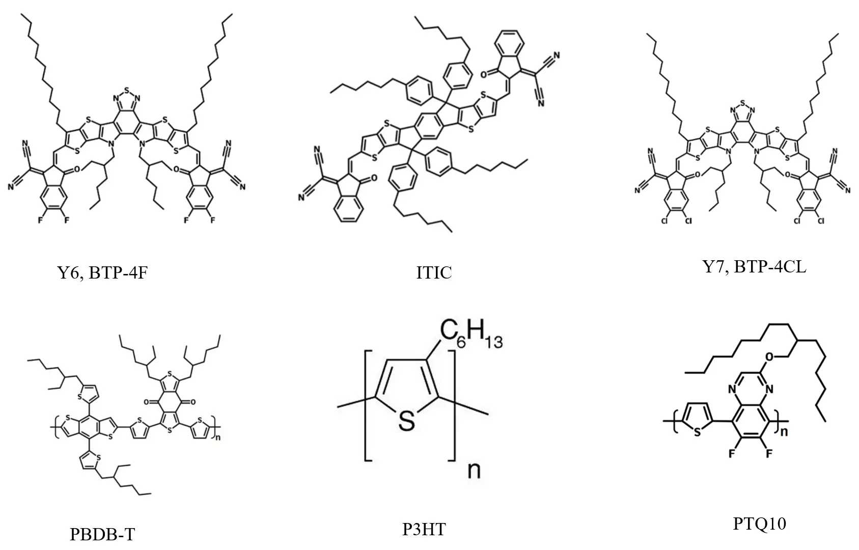
In this formula, Jsc indicates the photocurrent produced with no voltage applied, Voc is the highest voltage possible when there is no load, and FF assesses the quality of the current-voltage characteristics. Together, these factors influence device efficiency and are discussed in this review regarding photonic and charge-transport improvement. Recent breakthroughs, especially in the development of high-performance non-fullerene acceptors (NFAs), have led to impressive advancements, with lab-reported efficiencies for single-junction OSCs surpassing 20% PCE [6]. Figure 1 shows molecular structures of some well-known donors and acceptors.
Recent efficiency breakthroughs exceeding 20% PCE in single-junction OSCs are primarily attributed to advances in active-layer morphology control and energetic optimization rather than optical enhancement alone. Jiang et al. demonstrated that incorporating a low-bandgap guest non-fullerene acceptor into a ternary blend enables finer phase separation and reduced energetic disorder, thereby suppressing non-radiative recombination while maintaining favorable charge-transport pathways. This strategy preserves open-circuit voltage while simultaneously enhancing photocurrent generation, thereby enabling certified efficiencies beyond 20% without introducing significant voltage loss [7]. However, despite these achievements, single-junction OSCs still face challenges like low absorption in small active layers, high charge recombination losses, and stability issues in real-world settings [8]. To tackle these challenges, researchers have explored photonics- and nanophotonics-based methods to improve the performance of single-junction OSCs. Techniques such as plasmonic nanostructures, photonic crystals, optical microcavities, and nanostructured interfaces are among the most promising approaches to enhance light trapping. These methods can increase the effective optical path length in thin active layers while improving charge transport and extraction efficiency [9]. A close look at these developments shows that computational modeling and targeted photonic engineering are not only helpful but also essential for enhancing the stability, efficiency, and eventual commercial success of single-junction OSCs. The primary goal of this review is to offer a thorough summary of photonics-based methods for light trapping and enhancing charge transport in OSCs. This study highlights the role of nanophotonic engineering in overcoming efficiency barriers by examining recent advancements in plasmonic nanostructures, photonic crystals, nanostructured transparent electrodes, and computational modeling. Furthermore, we discuss experimental validation and identify important future directions for improving OSC stability, efficiency, and large-scale integration. By enhancing light absorption and charge mobility, integrating photonic and nanophotonic structures into OSCs positions competitively alongside second-generation photovoltaic technologies, according to our findings. While this review focuses on single-junction OSCs for a detailed analysis of nanophotonic strategies, it is important to acknowledge that tandem or multijunction OSC architectures also show great potential for achieving higher theoretical efficiencies [10]. By stacking complementary absorbers, tandem devices can better utilize the solar spectrum, pushing certified PCE values beyond 20–25% [11]. Zhu et al. reported a record single-junction OSC efficiency of approximately 20.8% by employing additive-assisted layer-by-layer fabrication to construct a bulk p–i–n architecture with improved thickness tolerance. This approach enables more uniform vertical phase distribution and optimized charge transport pathways, thereby reducing bimolecular recombination and resistive losses while maintaining strong optical absorption in thick active layers [12]. Similarly, Chen et al. achieved efficiencies approaching 21% through a diluted ternary heterojunction strategy that finely tunes nanoscale morphology and suppresses charge recombination. By introducing a minor third component to regulate donor–acceptor packing and energetic alignment, this design simultaneously enhances carrier lifetime and charge extraction efficiency, leading to record-level performance without compromising device stability [13]. However, tandem OSCs introduce additional complexity in optical management, layer alignment, and interfacial engineering, which are outside the scope of this work. The insights gained from optimizing single-junction devices will still be crucial for future tandem device designs. While photonic design is often discussed primarily in the context of light trapping, its impact on charge transport processes is equally important for achieving high device performance. Nanophotonic structures not only enhance optical absorption but also modify local electric fields, exciton generation profiles, and interfacial energetics, thereby influencing charge separation, recombination, and carrier extraction. In this review, photonic enhancement strategies are therefore examined from a dual perspective, considering their coupled effects on both optical management and charge transport optimization in single-junction organic solar cells.
2. Light-Trapping Mechanisms in Single-Junction Organic Solar Cells
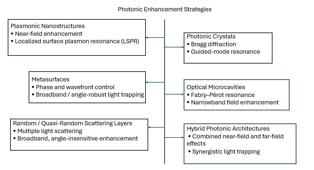
Single-junction OSCs have optical limits due to their thin active layers, typically 100–300 nm [14]. Thin-film structures facilitate efficient extraction and offer mechanical flexibility, but they limit light absorption, particularly in the near-infrared range. This limitation restricts the potential PCE. To address this issue, researchers have developed various specialized light-trapping strategies for single-junction OSC designs. Instead of increasing the thickness of the active layer, which could lead to increased recombination losses, these light management techniques focus on extending the effective optical path length within the absorber layer. Important strategies include using plasmonic nanogratings, which are periodic metallic nanostructures that harness localized surface plasmon resonances (LSPRs) to boost and concentrate the electromagnetic field near the device surface, thereby improving light absorption and strengthening the local electromagnetic field [15]. Figure 2 shows the classification of photonic enhancement strategies in single-junction OSCs.
Other strategies involve photonic crystals, which manipulate light through Bragg diffraction and guided-mode resonances [16], metasurfaces, designed at the subwavelength scale to widen the angular and spectral response [17], and optical microcavities, which use constructive interference to enhance internal photon recycling [18]. These nanophotonic strategies not only improve absorption but also provide additional benefits by increasing exciton generation, decreasing charge recombination, and enabling better carrier extraction. Recent studies show that incorporating plasmonic elements or photonic back reflectors increases Jsc and can also improve Voc and FF, thereby enhancing PCE in single-junction devices [19,20]. Furthermore, hybrid designs that combine photonic crystals with embedded plasmonic nanoparticles show promise for capturing a broader portion of the solar spectrum, extending from the visible to the near-infrared region [21]. Table 1 summarizes recent advancements related to single-junction OSCs and highlights the progress achieved through these innovative photonic and nanophotonic strategies.
Table 1. Recent advancements in light-trapping techniques for single-junction organic solar cells.
|
Strategy |
Physical Mechanism |
Typical Performance Enhancement |
|---|---|---|
|
SiO2-coated Ag nanoparticles |
LSPR-induced near-field enhancement |
|
|
2D photonic crystal back reflectors |
Bragg diffraction, guided-mode resonance |
|
|
Plasmonic rear reflectors |
Surface plasmon polariton coupling |
|
|
Nanostructured dielectric reflectors |
Photon recycling, optical path extension |
|
|
Quantum dot integration |
Spectral extension into NIR |
2.1. Plasmonic Nanostructures for Light Absorption Enhancement
Plasmonic nanostructures, especially those made of noble metals such as silver (Ag) and gold (Au), have been widely studied to enhance light absorption in single-junction OSCs [27]. These structures use LSPR to boost the intensity of the electromagnetic field close to the nanoparticle surface [28]. This increase raises the chances of capturing photons within the thin active layer [29]. Plasmonic nanostructures are usually added to OSCs in various ways. They can be embedded in the active layer, placed at the donor-acceptor interface, or coated on charge transport layers. Each configuration seeks to maximize near-field enhancement while minimizing parasitic absorption losses [30]. For instance, the incorporation of Ag nanoparticles coated with a thin dielectric shell (e.g., SiO2) at the interface between the active layer and the hole transport layer has shown a Jsc increase of about 15 to 18% and a PCE improvement of roughly 12 to 16%, depending on the size and concentration of the nanoparticles [31]. However, plasmonic strategies come with trade-offs. While near-field effects can greatly improve absorption, too much metallic content can cause parasitic absorption losses and reduce device stability due to the oxidation and clumping of nanoparticles over time [32]. Recent progress has tried to address these issues by using hybrid plasmonic-dielectric structures or by using ultra-small, well-spread nanoparticles to find a balance between optical benefits and chemical stability [33]. Plasmonic nanostructures offer a promising option for enhancing absorption efficiency in single-junction OSCs, especially when there is careful control of nanoparticle size, distribution, and surface coating.
2.2. Photonic Crystals
Photonic crystals (PCs) are periodic structures made of dielectric materials that control light propagation through constructive and destructive interference. When designed correctly, these crystals can induce Bragg diffraction and guided-mode resonances, thereby improving light trapping in the active layer of organic solar cells [34]. These structures are especially useful for single-junction OSCs, where the thin active layer needs optical path enhancement to harvest enough photons. For instance, studies using nanoimprinted photonic crystal back reflectors under the active layer have shown improvements in the external quantum efficiency (EQE) of up to 30–40% in the 500–800 nm spectral range [35,36]. Correspondingly, single-junction OSCs integrating photonic crystal structures have reported Jsc enhancements of approximately 18–25%, resulting in overall PCE gains of 10–15% compared to flat-reference devices [31]. The fabrication of photonic crystals typically involves techniques such as nanoimprint lithography, interference lithography, or self-assembly, each offering varying degrees of pattern fidelity and scalability. While photonic crystals significantly improve light harvesting, they exhibit inherent angular sensitivity, meaning their light-trapping efficiency can decline under off-normal illumination conditions [37]. This limitation has spurred recent research into quasi-random photonic crystals and chirped structures to broaden the angular and spectral response.
2.3. Metasurfaces
Metasurfaces are two-dimensional arrays of tiny nanostructures designed to control the amplitude, phase, and polarization of incoming light with great precision. In OSCs, metasurfaces are a powerful tool for managing light, improving photon collection over a wide range of wavelengths and angles [38]. By taking advantage of phase shifts at the nanoscale, metasurfaces can redirect and focus light into the thin active layers of single-junction OSCs. Unlike traditional plasmonic structures, metasurfaces allow for low-loss, broadband, and angle-independent light trapping, which is essential for sustaining high performance under varying solar conditions [39]. Recent studies have shown that adding dielectric or hybrid dielectric–metallic metasurfaces above or below the active layer can improve PCE by 3–5% compared to flat designs [40]. For example, integrating a dielectric metasurface grating into a polymer-based OSC boosted the Jsc by approximately 12% and increased PCE by about 4% [41]. Creating metasurfaces remains challenging despite their promising optical properties. Techniques like electron beam lithography (EBL) and focused ion beam (FIB) milling offer high precision but are slow and costly, which complicates large-scale production. Recent improvements in nanoimprint lithography and scalable colloidal lithography techniques present promising routes for cost-effective metasurface fabrication.
2.4. Optical Microcavities and Light Management Layers
Optical microcavities employ constructive interference to confine light within specific regions of the device stack, enhancing optical absorption and exciton generation. These cavities are typically formed between reflective interfaces, such as distributed Bragg reflectors (DBRs) and semitransparent electrodes, or via Fabry–Pérot-type resonators integrated directly into the device architecture [42]. In such structures, the optical path is effectively increased by resonant enhancement, with peak absorption occurring at cavity resonance wavelengths, typically tailored to the visible and near-infrared ranges depending on the active layer’s absorption spectrum. Recent studies have shown that incorporating optical microcavities can lead to PCE improvements of 15–20%, primarily due to improved light harvesting in specific spectral regions and the suppression of parasitic absorption in the charge transport layers [43]. For example, by adjusting the cavity length to match the quarter- or half-wavelength of target absorption peaks (e.g., 550–750 nm), internal photon density can be significantly amplified. High-index dielectric spacer layers, such as ZnO or TiO2, further modulate the phase of reflected light, optimizing interference conditions while simultaneously serving as electron transport layers. These strategies are especially effective in semitransparent and flexible OSC applications, where device thickness is constrained, and efficient light management is essential. Microcavities also play a critical role in tandem and multijunction OSCs, where spectral selectivity and interlayer optical control are key to achieving optimal subcell current matching [44]. However, a key limitation of microcavity-enhanced devices is their narrowband response: enhancement is strongest only at specific wavelengths and angles, which can reduce performance under diffuse or off-normal illumination conditions [45]. To address this, hybrid cavity systems incorporating photonic crystals or nanoscatterers have been explored, enabling broader angular respons and more uniform absorption enhancement across the solar spectrum [46]. Overall, optical microcavities provide a compact and tunable platform for improving light absorption in OSCs, particularly in applications that demand semitransparency or narrow spectral optimization, though trade-offs in bandwidth and fabrication complexity must be managed for broader deployment.
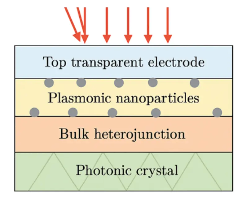
2.5. Synergistic Light-Trapping Strategies
Recent research shows that combining multiple light-trapping methods within a single OSC design can yield better performance than using each method alone [47]. These combined approaches leverage both near-field and far-field optical effects, thereby improving absorption across a wider range of wavelengths and under different lighting angles [48]. For instance, metasurfaces provide stability across angles, while photonic crystals offer wavelength selectivity. Their combination enhances absorption across a range of wavelengths and angles. Similarly, pairing plasmonic elements with dielectric microcavities allows for both field localization and resonance-based enhancement. This results in better optical confinement within the active layer [49], as shown in Figure 3. These mixed strategies also allow for adjustments through the optimization of design and material parameters, making them suitable for various OSC designs and material systems. Different light-trapping methods working together can greatly boost efficiency. For example, OSCs have reached PCE values over 20% by integrating plasmonic nanoparticles with photonic crystal back reflectors [50]. Hybrid metasurface and microcavity designs are advancing light management in OSCs, making them more competitive with traditional solar technologies [51]. Optical microcavities, metasurfaces, photonic crystals, and plasmonic nanostructures have all been successfully combined to enhance light absorption and charge generation in OSCs. Recent developments in these areas have led to significant efficiency gains; some designs have shown notable increases in Jsc and up to 50% more light absorption [52]. Looking ahead, improving these strategies through computer modeling and design will be essential for boosting OSC performance and commercial potential [53,54].
These comparative insights in Table 2 highlight that, while significant gains in light absorption and photocurrent generation have been achieved through advanced photonic structures, practical considerations, such as fabrication complexity, cost, angular robustness, and integration with flexible organic substrates, must guide the future design of scalable, high-efficiency single-junction OSCs.
Table 2. Comparative assessment of key photonic strategies applied in single-junction.
|
Strategy |
Typical Efficiency Gain |
Fabrication Complexity |
Cost |
Key Limitations |
|---|---|---|---|---|
|
Plasmonic |
Moderate (10–20%) |
Moderate (metal nanoparticle embedding or coating) |
High (precious metals) |
Parasitic absorption Losses, potential instability under illumination. |
|
High (20–40%) |
High (nanoimprint lithography, advanced etching) |
Moderate–High |
Angle sensitivity, integration challenges with flexible substrates. |
|
|
Metasurfaces |
Very High (>30%) |
Very High (electron beam lithography, complex patterning) |
High |
Difficult to scale up, expensive fabrication processes. |
|
Random Scattering |
Low–Moderate (5–15%) |
Low (solution processing, spin-coating) |
Low |
Limited broadband Enhancement, less spectral tunability. |
|
Optical Microcavities |
Moderate (10–25%) |
Medium (dielectric mirror deposition) |
Moderate |
Narrowband Enhancement |
2.6. Challenges and Limitations in Scaling Up Photonic Enhanced OSCs
While nanophotonic strategies have demonstrated significant performance enhancements in single-junction organic solar cells at the laboratory scale, their translation to large-area and commercially viable devices remains challenging. A primary limitation lies in the complexity and cost of fabrication, as many high-performance photonic structures rely on techniques such as electron-beam lithography, focused ion beam milling, or high-resolution nanoimprint lithography, which are inherently low-throughput and economically impractical for roll-to-roll manufacturing [65,66]. In addition, achieving uniform and reproducible nanostructure patterning across large device areas remains a critical challenge, as small variations in feature size, spacing, or alignment can lead to non-uniform optical responses and batch-to-batch performance fluctuations [67]. Another key concern is angular dependence: many periodic photonic structures exhibit optimal light trapping only under near-normal incidence, with efficiency diminishing under diffuse or off-normal illumination conditions commonly encountered in real-world operation [68,69]. Device stability further complicates commercialization, particularly for plasmonic architectures, where metallic nanostructures are susceptible to oxidation, agglomeration, and interfacial degradation under prolonged thermal and photochemical stress, adversely affecting long-term performance [70,71]. To mitigate these challenges, recent efforts have focused on scalable alternatives such as quasi-random nanostructures, hybrid organic–dielectric photonic designs, and computationally optimized nanophotonic architectures that balance optical enhancement with manufacturability and stability [72,73]. Collectively, these findings highlight that while photonic enhancement offers substantial efficiency gains, overcoming scalability, angular robustness, and durability constraints is essential for enabling the practical deployment of photonic-enhanced single-junction OSCs.
3. Nanophotonic Strategies for Charge Transport Optimization in OSCs
The achievement of high PCE in OSCs depends on effective charge transport. Beyond optical gains, photonic architectures can reshape charge transport pathways by altering carrier density distributions, recombination dynamics, and interfacial electric fields, making transport optimization an intrinsic component of photonic device design. Localized electronic states, high exciton binding energy, and recombination losses still cause charge carrier mobility in OSCs to be many orders of magnitude lower than in inorganic photovoltaics, even with advances in materials and device engineering [74]. Because of these problems, OSC systems are increasingly incorporating nanophotonic techniques to maximize charge transfer, reduce recombination losses, and increase carrier collection efficiency [75]. Charge transport layers, plasmonic-enhanced carrier extraction, nanostructured transparent electrodes, and dielectric interface engineering are the main areas of emphasis for these strategies. Figure 4 illustrates OSCs’ use of nanophotonic techniques.
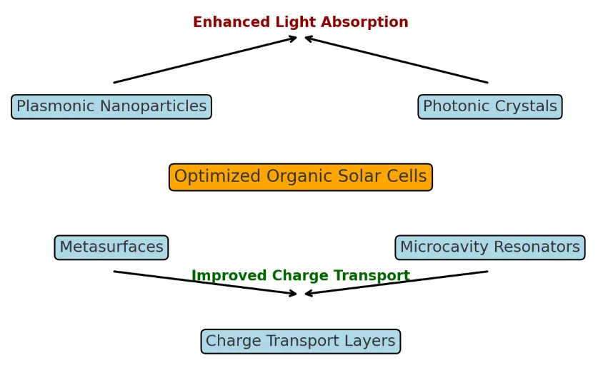
Figure 4. Schematic illustration of nanophotonic strategies in organic solar cells, highlighting how different photonic enhancements contribute to improved light absorption and charge transport efficiency.
3.1. Nanostructured Transparent Electrodes for Enhanced Carrier Extraction
Charge extraction requires transparent conductive electrodes (TCEs) that maintain high optical transparency. Indium tin oxide (ITO)-based conventional OSC electrodes are brittle and have low conductivity. Researchers have looked into nanostructured TCEs composed of graphene, metal mesh grids, and silver nanowires (AgNWs) to circumvent these restrictions [76].
-
-
AgNWs: AgNWs offer high conductivity and optical transparency while providing mechanical flexibility. Studies have shown that hybrid AgNW–graphene TCEs achieve higher charge extraction rates and lower series resistance, resulting in 8–12% PCE enhancement compared to conventional ITO-based OSCs [77].
-
-
Graphene-Based Electrodes: Graphene’s high carrier mobility and transparency make it an excellent candidate for replacing ITO. Recent work demonstrated that doped graphene sheets incorporated into the charge extraction layers led to a 20% reduction in charge recombination and improved FF values in OSCs [78].
-
-
Metal Mesh Electrodes: Nanoscale metal grids improve electrical conductivity while preserving high optical transmittance. Hybrid metal mesh ITO composites have been reported to improve carrier transport efficiency, leading to OSC efficiencies exceeding 20% [79].
3.2. Plasmonic-Enhanced Charge Transport and Recombination Suppression
It has recently been discovered that plasmonic effects, which are well known for improving light trapping, play a major role in optimizing charge transfer in OSCs [80]. NPs, especially those of gold (Au) and silver (Ag), minimize energy losses and increase device efficiency by producing localized electric fields that promote exciton dissociation and charge separation [81]. This LSPR effect improves light absorption and enhances carrier transport by reducing recombination rates. In addition, studies have demonstrated that incorporating Au nanorods into charge transport layers speeds up carrier extraction, resulting in a 30% decrease in recombination losses and a rise in PCE from 15% to 18% [82]. The near-field enhancement produced by these nanorods strengthens the built-in electric field, facilitating more efficient movement of charge carriers toward the electrodes. Plasmonic nanostructure insertion into high-k dielectric layers has been shown to significantly enhance energy level alignment in bulk heterojunction OSCs, thereby increasing charge mobility and decreasing trap-assisted recombination losses [83]. These advancements highlight the dual role of plasmonic engineering in both light management and charge transport optimization, making it a crucial strategy for next-generation OSCs.
3.3. Charge Transport Layer Engineering via Nanostructuring
An important factor in OSC efficiency is the properties of charge transport layers (CTLs), which facilitate the extraction and movement of charge carriers while blocking the flow of opposing charges. The recent improvements have focused on aligning the energy levels with the active layer, improving conductivity, and enhancing transparency in CTLs. For example, the creation of special hole-transporting layers with enhanced charge mobility and specific energy levels has greatly enhanced device operation. These developments raise the total PCE of OSCs by reducing charge recombination and raising fill factors [84]. To optimize charge dynamics, recent advancements in CTL have used nanostructuring techniques, including conductive polymers, quantum dots, and self-assembled monolayers (SAMs) [85]. It has been demonstrated that adding CdSe and PbS quantum dots as interfacial layers alters energy level alignments, improves charge transfer efficiency, and decreases interfacial defects, which raises Voc and decreases dark current [86]. SAM-functionalized ZnO layer integration has also been shown to be successful in lowering interfacial recombination: studies have reported improved device stability and a 10% increase in charge collection efficiency [87]. Conductive polymers, such as doped poly(3,4-ethylenedioxythiophene) polystyrene sulfonate (PEDOT:PSS), have also been widely used to improve hole extraction and reduce contact resistance at the anode. Recent research has demonstrated that PEDOT: PSS doped with MoS2 nanosheets enhances carrier mobility and boosts PCE by ~2–3% [88]. The combined use of these nanostructured CTLs not only improves charge transport pathways but also enhances device longevity, making them crucial for the development of stable high-performance OSCs.
3.4. Dielectric Interface Engineering for Optimized Charge Transport
Dielectric engineering involves modifying dielectric layer properties, such as permittivity and energy-level alignment, to optimize charge-carrier extraction and suppress interfacial recombination losses. It is essential to enhance carrier extraction and transport dynamics, in addition to altering charge-transport layers [89]. Enhancing carrier injection efficiency and decreasing charge accumulation at interfaces are two benefits of using high-k materials (such as TiO2 and HfO2) as buffer layers [90]. It has been demonstrated that TiO2 interlayers increase electron transport rates, stabilizing device performance over 1000 operating hours. Researchers have effectively adjusted the inherent electric field by adding molecular dipole layers at the metal organic interface, improving hole extraction efficiency [91]. According to studies, interface dipole layers increase FF values by approximately 15% by improving charge selectivity [92].
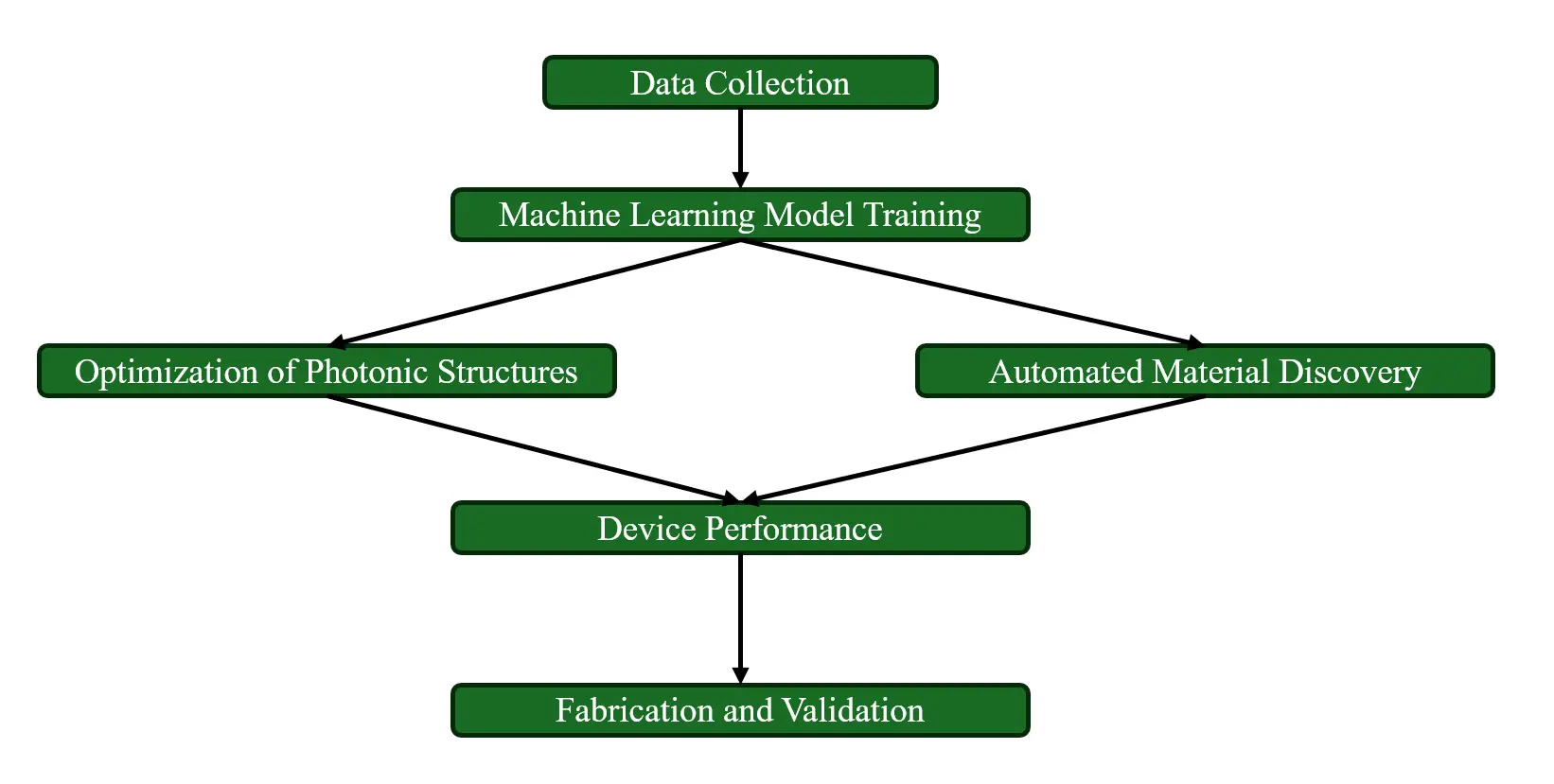
4. Computational and Theoretical Advances in Photonics-Enhanced Organic Solar Cells
All device performance metrics, including PCE, Jsc, and EQE, are reported under standard AM1.5G illumination (100 mW/cm2) unless otherwise specified. Photonics-enhanced OSCs are largely designed and optimized through theoretical simulations and computational modeling. Researchers can anticipate charge transport behavior, evaluate light matter interactions, and optimize nanophotonic structures for increased PCE thanks to these methods [93,94]. Through the integration of machine learning algorithms, density functional theory (DFT), drift diffusion modeling, and finite difference time domain (FDTD) simulations, computational methods aid in determining the most effective OSC topologies and directing experimental fabrication [95]. In this section, we provide a detailed overview of the computational modeling and optimization strategies that have become critical for the rational design of photonic structures in organic solar cells in Figure 5.
4.1. Finite-Difference Time-Domain (FDTD) Simulations for Light Trapping Optimization
Light absorption in OSCs and electromagnetic wave propagation modeling are two typical applications of FDTD. To ascertain their effect on light trapping efficiency, it enables accurate simulations of optical microcavities (which utilize resonance effects between reflective layers to confine photons within the active layer, thus extending their optical path and improving absorption efficiency), photonic crystals, and plasmonic nanostructures [96]. According to recent research, adding nanostructured metal back reflectors increases light absorption and raises Jsc by 25% in FDTD simulations [97]. Furthermore, it has been shown that FDTD-based modification of plasmonic nanoparticles embedded in charge-transport layers significantly improves overall OSC performance and exciton dissociation rates [98].
4.2. Drift-Diffusion Modeling for Charge Transport Analysis
Charge carrier mobility, recombination rates, and dynamics in OSCs can be thoroughly examined using drift-diffusion models. Device topologies can be optimized for reduced recombination losses and increased carrier collection efficiency by using these models to simulate carrier transport under different electric fields [99]. Changing the alignment of the energy level at donor acceptor interfaces can increase the efficiency of charge extraction by up to 30%, according to advanced drift-diffusion simulations, including trap-assisted recombination models [100]. Enhancing the performance of bulk heterojunction OSCs and ensuring stability over time requires this knowledge.
4.3. Density Functional Theory (DFT) for Material Screening
Novel organic semiconductor materials with optimum energy band alignment, exciton binding energies, and charge mobility can be found with DFT-based computations [101]. DFT predicts the effect of molecular packing on charge transport and offers insights into exciton dissociation efficiency by assessing donor-acceptor interactions at the molecular level [102]. High-efficiency NFAs for OSCs, regarding recent developments in hybrid DFT approaches, have made it possible to forecast charge injection barriers and trap-state density with greater accuracy [103].
4.4. Machine Learning and AI Optimization
Machine learning (ML) algorithms and artificial intelligence (AI) are revolutionizing photonic design and material selection in OSCs. Neural networks and genetic algorithms are data-driven techniques that allow researchers to predict optimal nanophotonic structures and processing conditions for enhanced efficiency [104]. Through AI-assisted plasmonic nanostructure optimization, self-assembled metasurfaces that maximize light absorption and reduce optical losses have been discovered. Because machine learning models based on experimental datasets may accurately predict device degradation mechanisms, it is possible to design OSCs that are more durable and resilient [105]. Computational and theoretical approaches, including FDTD simulations, drift diffusion modeling, DFT calculations, and AI optimization, have significantly contributed to the advancement of photonics-enhanced OSCs. These methods provide valuable insights into light trapping, charge transport mechanisms, and material design, leading to the development of stable high-efficiency OSC architectures. Moving forward, integrating multi-scale modeling techniques with experimental validation will be essential to further improve OSC performance and accelerate commercialization [106].
5. Experimental Validation of Photonic Enhancements in Organic Solar Cells
Experimental validation is essential to evaluate the efficacy of photonic and nanophotonic techniques in OSCs. Experimental methods verify these gains through fabrication, optical characterization, and electrical performance analysis, even if theoretical models predict improvements in light trapping, charge transport, and efficiency [107]. Techniques including ultraviolet-visible (UV-Vis) spectroscopy, EQE measurements, and impedance spectroscopy have been used to experimentally test recent developments in plasmonic nanostructures, photonic crystals, and metasurfaces [108].
5.1. Optical Characterization of Light-Trapping Strategies
Light-trapping devices such as microcavity resonators, photonic crystals, and plasmonic nanoparticles have been thoroughly investigated using optical characterization approaches. UV-Vis spectroscopy measures the increased absorption spectra resulting from nanophotonic changes. Studies incorporating plasmonic nanoparticles have demonstrated 15–25% absorption enhancement in the visible spectrum [109]. EQE determines how effectively absorbed photons contribute to the photocurrent. OSCs with metasurface-based light management layers have exhibited EQE enhancements of 20–30% compared to conventional devices [110]. Near-field optical microscopy (NSOM) provides spatial resolution of light-matter interactions at the nanoscale. NSOM studies confirm the localized field enhancement around plasmonic nanoparticles, directly correlating with improved charge generation [111]. These computational approaches-including electromagnetic simulations, quantum mechanical calculations, and AI modeling-are now central pillars in developing high-performance, scalable, and photonic-enhanced OSC architectures [112].
5.2. Electrical Performance Analysis of Charge Transport Enhancements
Using electrical characterization approaches, experimental evaluations concentrate on device efficiency, charge carrier mobility, and recombination losses to verify the efficacy of nanophotonic charge transport strategies. Measurements are taken of Current-Voltage (J-V) yield Voc, Jsc, and FF. OSCs integrating plasmonic-enhanced charge transport layers have shown PCE improvements of 3–5% due to enhanced carrier extraction [113]. Impedance spectroscopy analyzes charge recombination dynamics and transport resistance. The experimental results indicate that plasmonic nanorods embedded in charge transport layers reduce recombination losses by 20–30%, leading to improved charge mobility [114]. Transient photovoltage and photocurrent measurements assess carrier lifetimes and extraction efficiency. Studies have demonstrated that hybrid plasmonic-dielectric interfaces enhance charge lifetimes by up to 35%, thereby contributing to more stable OSC performance [115] (Figure 6).
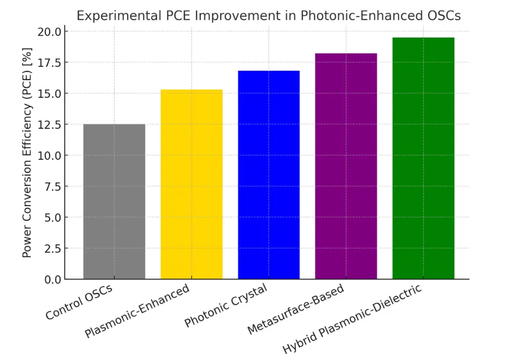
Figure 6. PCE improvements in OSCs with different photonic enhancements. The chart compares conventional OSCs with plasmonic, photonic crystal, metasurface, and hybrid plasmonic–dielectric designs based on experimental validation.
5.3. Stability and Long-Term Performance Testing
Photonic-enhanced OSCs need to show operational stability for practical uses in addition to efficiency gains. Accelerated aging tests are experiments that assess how a gadget deteriorates when exposed to constant changes in temperature, humidity, and light. OSCs with photonic crystal back reflectors exhibit 20% longer operational lifetimes due to improved thermal stability [116]. Encapsulation studies assess moisture resistance for long-term stability. Studies indicate that plasmonic nanostructures can mitigate oxygen-induced degradation, preserving OSC performance over extended periods [117]. Light absorption, charge transfer, and stability in OSCs are greatly enhanced by photonic and nanophotonic enhancements, as demonstrated by experimental confirmation. Electrical performance studies demonstrate improved charge extraction and decreased recombination losses, while optical characterizations confirm increased absorption and exciton formation. Additionally, stability tests show that photonic-engineered OSCs have longer operational lifespans, making them suitable for commercial use.
6. Current Challenges in Achieving High PCE and Stability
Despite quick advancements in material design, photonic engineering, and device structure, it is still tough to achieve high PCE and long-term stability in single-junction OSCs. These challenges come from a mix of photophysical losses, charge transport issues, material instability, and manufacturing limits. Together, these factors prevent high-performance lab devices from becoming commercially viable technologies [118]. A major efficiency hurdle in OSCs is non-radiative recombination, which is especially noticeable in narrow-bandgap donor-acceptor systems made to extend light absorption into the near-infrared range. While these materials can boost Jsc, they often face increased energetic disorder and trap-assisted recombination, which lowers Voc [119]. Reducing these losses requires careful control over molecular packing, energy alignment, and the presence of defects at interfaces. Exciton dissociation and charge separation also pose challenges because of the naturally short exciton diffusion lengths in organic semiconductors. Poorly functioning donor-acceptor interfaces and less-than-ideal nanoscale structures can lead to significant recombination before creating free charge carriers, which limits photocurrent. Although nanophotonic techniques improve exciton generation by enhancing light absorption, they don’t automatically address interfacial recombination losses, underscoring the need to optimize both optical and electronic processes simultaneously. Device stability is a major barrier to commercialization. OSCs are very sensitive to environmental factors like oxygen, moisture, thermal changes, and ultraviolet light. Degradation processes, such as donor-acceptor phase separation, electrode diffusion, and chemical reactions at interfaces, can degrade performance over time. Even when initial PCEs are above 20%, keeping devices operating steadily for a long time is difficult without high-quality encapsulation and robust material systems. Limitations in charge transport further hold back device performance. The low carrier mobility of organic materials, along with structural disorder in bulk heterojunctions, hinders efficient charge collection and raises series resistance. Cutting through this challenge requires finding a good balance between phase separation for exciton dissociation and percolation pathways for charge transport. On top of that, mismatches in energy levels at transport-layer interfaces can create additional recombination paths and increase losses during extraction. Design limitations also matter significantly. It is crucial to optimize transport layers, transparent conductive electrodes, and metal contacts to ensure balanced extraction of electrons and holes. However, improving one aspect often entails trade-offs in optical transparency, mechanical flexibility, or stability, complicating the optimization of single-junction devices.
Lastly, scalability and cost are ongoing challenges. Many high-efficiency OSCs depend on complex material creation, precise thickness control, and fabrication processes that don’t work well with roll-to-roll manufacturing. As device sizes grow, problems such as film uniformity, resistive losses, and tolerance to defects become more evident. Therefore, creating affordable materials, scalable application methods, and robust device designs is essential for turning lab progress into commercially viable OSC technologies.
Impact of Photonic Structures on Device Stability
While photonic and nanophotonic structures have been widely used to improve light absorption and photocurrent generation in single-junction OSCs, their effects on long-term device stability add complexity that requires careful examination. In addition to optical improvements, photonic designs can change local thermal profiles, interfacial chemistry, and mechanical stress distribution within the device stack. These changes can influence degradation pathways during operation. Metallic plasmonic nanostructures, especially those made from silver and gold, are some of the most studied photonic improvements. However, their integration can lead to stability issues due to localized plasmon-induced heating, metal diffusion, and oxidation under extended illumination and thermal stress. These factors can accelerate photo-oxidative degradation of organic active layers and charge-transport interfaces, leading to a more rapid decline in efficiency despite initial performance gains. Encapsulating metallic nanoparticles with dielectric shells, like SiO2 or Al2O3, and keeping them isolated from the active layer can help reduce chemical reactivity and limit thermal hotspots [120]. Dielectric photonic structures, such as photonic crystals and metasurfaces made from oxides or polymer materials, usually provide better chemical stability than metallic ones. However, using these structures can increase interfacial roughness, mechanical stress, or pathways that allow moisture to enter, especially in flexible and large-area devices [121]. In some cases, nano-patterned interfaces can worsen morphological instability in bulk heterojunction layers, indirectly affecting charge transport and speeding up degradation under cyclical thermal or mechanical stress. Optical microcavities and resonant light-management layers add more challenges for stability. While microcavities enhance absorption through constructive interference, their narrowband and uneven optical benefits can cause localized heating and non-uniform aging across the device [122]. Recent studies show that broadband cavity designs and thermally durable dielectric spacers can help improve these issues, enhancing operational stability without losing optical performance [123]. To tackle these challenges, new strategies increasingly focus on designing photonic structures alongside materials and device designs aimed at stability. This includes replacing metallic plasmonic components with low-loss dielectric resonators, integrating photonic features into charge-transport layers rather than the active layer, and combining photonic improvements with advanced encapsulation methods [124]. Overall, these approaches highlight the need to pursue photonic enhancement and stability optimization together. A solid understanding of how photonic designs interact with degradation mechanisms is crucial for advancing photonic-enhanced OSCs from lab tests to lasting, commercially viable technologies.
The following Table 3 shows the stability of photonic enhancement strategies in single-junction OSC.
Table 3. Stability implications of photonic enhancement strategies in single-junction OSCs.
|
Photonic Strategy |
Primary Stability Concern |
Underlying Mechanism |
Reported Mitigation Strategies |
|---|---|---|---|
|
Plasmonic nanoparticles |
Accelerated degradation and PCE decay |
Localized surface plasmon resonance (LSPR) induces nanoscale thermal hotspots that accelerate polymer photo-oxidation; oxidation and diffusion of metal nanoparticles (Ag/Au) into adjacent organic layers introduce non-radiative recombination centers and interfacial defects during prolonged illumination. |
Dielectric shell coating (e.g., SiO2), spatial isolation from the active layer, reduced nanoparticle loading density. |
|
Photonic crystal back reflectors |
Mechanical and interfacial instability |
Periodic surface topography increases surface roughness and induces localized stress concentration during thermal cycling and mechanical bending; rough interfaces weaken adhesion between photonic crystal layers and organic transport layers, promoting delamination, crack formation, and interfacial failure over time. |
Polymer-compatible nanoimprinting, planarization interlayers, mechanically compliant buffer layers. |
|
Metasurfaces |
Fabrication-induced defects and long-term reliability issues |
High-resolution nanoscale patterning (e.g., EBL, FIB) introduces edge defects and surface states that act as charge trapping sites and pathways for moisture ingress, increasing susceptibility to electrical breakdown and environmental degradation. |
Dielectric metasurfaces, hybrid photonic designs, scalable low-damage patterning methods (e.g., nanoimprint lithography). |
|
Optical microcavities |
Localized heating and non-uniform aging |
Resonant optical confinement produces spatially non-uniform photon density and localized electromagnetic field maxima (antinodes), leading to uneven photothermal stress and accelerated degradation in high-field regions under continuous illumination. |
Broadband cavity designs, optimized cavity thickness, high-index dielectric spacers to distribute optical fields more uniformly. |
|
Hybrid photonic–dielectric structures |
Interfacial compatibility and processing-induced stress |
Thermal expansion mismatch and surface energy incompatibility between organic semiconductors and inorganic dielectric layers generate interfacial stress and defect formation; multi-step processing increases residual stress and encapsulation complexity. |
Solution-processed dielectric layers, interface engineering, improved encapsulation strategies. |
7. Future in Photonics-Driven Organic Solar Cells
The future developments in photonics-driven OSCs will concentrate on resolving issues with stability, efficiency, and large-scale manufacturing. The integration of metasurfaces, quantum dots, and plasmonic nanostructures to enhance exciton production and photon harvesting is an emerging approach for light trapping [125]. When QDs are used in active layers, the spectral response is extended to the near-infrared region, increasing Jsc by 15–20%. Further closing the performance gap between OSCs and conventional silicon photovoltaics are hybrid perovskite-organic tandem cells with photonic crystal back reflectors, which have been claimed to attain record-breaking efficiencies above 24% [126]. For designing photonic OSCs and material selection, the use of AI and ML is revolutionary. AI algorithms can analyze large datasets to predict the optimal nanophotonic designs, reducing fabrication time and costs while boosting efficiency. According to recent research, photonic engineering can improve light absorption, reduce parasitic losses, and optimize nanostructured electrodes, thereby increasing the efficiency of charge transport [127]. Furthermore, the optimization of the encapsulation layer using reinforcement learning techniques has resulted in a 40% increase in device life in real-world scenarios.
Enhancing charge transport, stability, and energy-level alignment is made possible by hybrid material integration, especially the use of perovskites and metal-organic frameworks (MOFs). As transparent conductive electrodes, MoS2 and WS2 have been used to replace ITO while retaining high transparency due to their better carrier mobility and hole extraction efficiency [128]. Moreover, donor-acceptor charge transfer has been enhanced by MOFs with adjustable band gaps, which have been effectively used to prolong OSC operational lifetimes and reduce recombination losses by 20% [129]. Despite these advances, scalability remains a major challenge for commercial deployment. Researchers are exploring R2R printing techniques and nanoimprint lithography for the large-scale fabrication of photonic-enhanced OSCs. Recent developments in self-assembled photonic crystal layers using printable materials have improved PCE by 18% while maintaining low production costs. Additionally, devices have demonstrated stability for more than 10,000 h under continuous illumination, with encapsulation techniques that use thin-film protective layers [130]. Unlocking the full potential of OSCs will require a multidisciplinary strategy that combines computational modeling, advanced photonics, and scalable production processes. It is anticipated that OSC technology will become more commercially viable through the integration of design, perovskite-organic hybrids, and R2R manufacturing. To ensure that photonics-driven OSCs are a significant part of the next generation of sustainable energy solutions, further research should focus on improving stability, enabling cost-effective large-scale production, and assessing the environmental consequences of OSC production. As OSC technology moves closer to commercialization, addressing environmental sustainability becomes increasingly critical [131]. Unlike traditional silicon photovoltaics, OSCs offer advantages such as low-temperature processing, reduced material usage, and the potential for scalable, low-energy roll-to-roll manufacturing. However, certain materials currently used in photonic enhancements, such as heavy metals (e.g., silver and gold), pose environmental and recycling challenges. Research into eco-friendly alternatives, including carbon-based plasmonic materials, biodegradable polymers, and green solvent systems, is gaining momentum. Furthermore, designing OSCs with end-of-life recyclability in mind, through modular device architectures and solvent-soluble interlayers, will be key to minimizing lifecycle environmental impacts and achieving truly sustainable photovoltaic technologies [132].
8. Conclusions
Light trapping, charge transfer, and overall device stability have all improved dramatically as a result of the combination of computational and nanophotonic techniques. Photonic strategies such as plasmonic nanostructures, photonic crystals, metasurfaces, and optical microcavities have enhanced photon harvesting, facilitated exciton dissociation, and reduced recombination losses, collectively contributing to record-breaking power conversion efficiencies. Concurrently, the development of high-performance materials has been accelerated, charge-transport behavior has been predicted, and nanophotonic geometries have been optimized, thanks in large part to computational modeling. Precise control over optical and electrical properties is now possible due to sophisticated simulations, machine learning, and optimization. These technologies have also facilitated the development of materials and structures that enhance stability and long-term performance. Despite these achievements, challenges persist. Scalability, cost-effective manufacturing, and environmental stability are among the challenges before the commercial readiness of photonic-enhanced OSCs. Future efforts should focus on R2R-compatible nanofabrication, robust thin-film encapsulation, integration of high-mobility transport layers, and exploration of tandem configurations, especially those combining organic and perovskite materials. Embracing green manufacturing practices and recyclable components will be essential for sustainable deployment. As we look to the future, the combination of scalable production techniques, material design, and self-assembled nanophotonic structures will allow the next generation of OSCs to surpass the lab-scale demonstrations. With these developments, photonic-enhanced OSCs are positioned as a vital technology in the global shift to renewable energy systems and as a strong substitute for traditional photovoltaics.
Statement of the Use of Generative AI and AI-Assisted Technologies in the Writing Process
During the preparation of this manuscript, the authors used Grammarly and GPT in order to correct writing and drafting. After using this tool, the authors reviewed and edited the content as needed and take full responsibility for the content of the published article.
Author Contributions
Conceptualization, M.S.H. and S.Y.F.; literature survey and analysis, M.S.H.; writing—original draft preparation, M.S.H.; writing—review and editing, M.S.H. and S.Y.F.; visualization, M.S.H.; supervision, S.Y.F.
Ethics Statement
Not applicable.
Informed Consent Statement
Not applicable.
Data Availability Statement
Data is available upon request.
Funding
This research received no external funding.
Declaration of Competing Interest
The authors declare that they have no known competing financial interests or personal relationships that could have appeared to influence the work reported in this paper.
References
- Brabec CJ, Scherf U, Dyakonov V. Organic Photovoltaics: Materials, Device Physics, and Manufacturing Technologies; John Wiley & Sons: Hoboken, NJ, USA, 2011. [Google Scholar]
- Li G, Zhu R, Yang Y. Polymer Solar Cells. Nat. Photonics 2012, 6, 153–161. DOI:10.1038/nphoton.2012.11 [Google Scholar]
- Hou J, Inganäs O, Friend RH, Gao F. Organic Solar Cells Based on Non-Fullerene Acceptors. Nat. Mater. 2018, 17, 119–128. DOI:10.1038/nmat5063 [Google Scholar]
- Yuan J, Zhang Y, Zhou L, Zhang G, Yip H-L, Lau T-K, et al. Single-Junction Organic Solar Cell with Over 15% Efficiency Using a Fused-Ring Acceptor with Electron-Deficient Core. Joule 2019, 3, 1140–1151. DOI:10.1016/j.joule.2019.01.004 [Google Scholar]
- Liu Q, Jiang Y, Jin K, Qin J, Xu J, Li W, et al. 18% Efficiency Organic Solar Cells. Sci. Bull. 2020, 65, 272–275. DOI:10.1016/j.scib.2020.01.001 [Google Scholar]
- Garnett EC, Ehrler B, Polman A, Alarcon-Llado E. Photonics for Photovoltaics: Advances and Opportunities. ACS Photonics 2020, 8, 61–70. DOI:10.1021/acsphotonics.0c01045 [Google Scholar]
- Jiang Y, Liu K, Liu F, Ran G, Wang M, Zhang T, et al. 20.6% Efficiency Organic Solar Cells Enabled by Incorporating a Lower Bandgap Guest Nonfullerene Acceptor Without Open-Circuit Voltage Loss. Adv. Mater. 2025, 37, e2500282. DOI:10.1002/adma.202500282 [Google Scholar]
- Li S, Fu Q, Meng L, Wan X, Ding L, Lu G, et al. Achieving over 18% efficiency organic solar cell enabled by a ZnO‐based hybrid electron transport layer with an operational lifetime up to 5 years. Angew. Chem. Int. Ed. 2022, 61, e202207397. DOI:10.1002/ange.202207397. [Google Scholar]
- Saeidi C, Weide DV. Wideband plasmonic focusing metasurfaces. Appl. Phys. Lett. 2014, 105, 053107. DOI:10.1063/1.4892560 [Google Scholar]
- Choudhury BD, Ibarra B, Cesano F, Mao Y, Huda MN, Chowdhury AR, et al. The photon absorber and interconnecting layers in multijunction organic solar cell. Sol. Energy 2020, 201, 28–44. DOI:10.1016/j.solener.2020.02.035 [Google Scholar]
- Mongia RK. Theoretical and experimental resonant frequencies of rectangular dielectric resonators. IEEE Proc. H 1992, 139, 98–104. DOI:10.1049/IP-H-2.1992.0016 [Google Scholar]
- Zhu L, Zhang M, Zhou G, Wang Z, Zhong W, Zhuang J, et al. Achieving 20.8% Organic Solar Cells via Additive-Assisted Layer-by-Layer Fabrication with Bulk p-i-n Structure and Improved Optical Management. Joule 2024, 8, 3153–3168. DOI:10.1016/j.joule.2024.08.001 [Google Scholar]
- Wang L, Chen C, Gan Z, Cheng J, Sun Y, Zhou J, et al. Diluted Ternary Heterojunctions to Suppress Charge Recombination for Organic Solar Cells with 21% Efficiency. Adv. Mater. 2025, 37, 2419923. DOI:10.1002/adma.202419923 [Google Scholar]
- Sun B, Lu H, Yang D, Long G, Zhang HL, Xue D. Magnetic Organic-Inorganic Hybrid Halide Perovskites: Fundamental Physics, Properties, and Applications. ACS Nano. 2025, 19, 22576–22599. DOI:10.1021/acsnano.5c02685 [Google Scholar]
- Catchpole KR, Polman A. Design Principles for Particle Plasmon Enhanced Solar Cells. Appl. Phys. Lett. 2008, 93, 191113. DOI:10.1063/1.3021072 [Google Scholar]
- Mokkapati S, Catchpole KR. Nanophotonic Light Trapping in Solar Cells. J. Appl. Phys. 2012, 112, 101101. DOI:10.1063/1.4747795 [Google Scholar]
- Khorasaninejad M, Capasso F. Metalenses: Versatile Multispectral Photonic Devices. Science 2017, 358, eaam8100. DOI:10.1126/science.aam8100 [Google Scholar]
- Hsiao YS, Charan S, Wu FY, Chien FC, Chu CW, Chen P, et al. Improving the light trapping efficiency of plasmonic polymer solar cells through photon management. J. Phys. Chem. C 2012, 116, 20731–20737. DOI:10.1021/jp306124n [Google Scholar]
- Ferry VE, Sweatlock LA, Pacifici D, Atwater HA. Plasmonic Nanostructure Design for Efficient Light Coupling into Solar Cells. Nano Lett. 2008, 8, 4391–4397. DOI:10.1021/nl8022548 [Google Scholar]
- Narasimhan VK, Cui Y. Nanostructures for photon management in solar cells. Nanophotonics 2013, 2, 187–210. DOI:10.1515/nanoph-2013-0001 [Google Scholar]
- Li X, Choy WC, Huo L, Xie F, Sha WE, Ding B, et al. Dual plasmonic nanostructures for high performance inverted organic solar cells. Adv. Mater. 2012, 24, 3046–3052. DOI:10.1002/adma.201200120 [Google Scholar]
- Atwater HA, Polman A. Plasmonics for Improved Photovoltaic Devices. Nat. Mater. 2010, 9, 205–213. DOI:10.1038/nmat2629 [Google Scholar]
- Branker K, Pathak MJ, Pearce JM. A review of solar photovoltaic levelized cost of electricity. Renew. Sustain. Energy Rev. 2011, 15, 4470–4482. DOI:10.1016/j.rser.2011.07.104 [Google Scholar]
- Spinelli P, Polman A. Light Trapping in Thin Crystalline Silicon Solar Cells Using Surface Mie Scatterers. IEEE J. Photovolt. 2014, 4, 554–559. DOI:10.1109/JPHOTOV.2013.2292744 [Google Scholar]
- Van de Hulst HC. Multiple Light Scattering: Tables, Formulas, and Applications; Elsevier: Amsterdam, The Netherlands, 2012. Available online: https://books.google.com.hk/books?hl=en&lr=&id=xeAkNn1ZBIwC&oi=fnd&pg=PP1&dq=25.%09Van+de+Hulst,+H.+C.+(2012).+Multiple+light+scattering:+tables,+formulas,+and+applications.+Elsevier.+&ots=oB8cD08UY3&sig=bcku_AzhpatmuA1ADUfdVSoTulk&redir_esc=y#v=onepage&q&f=false (accessed on 1 November 2025).
- Erwin WR, Zarick HF, Talbert EM, Bardhan R. Light trapping in mesoporous solar cells with plasmonic nanostructures. Energy Environ. Sci. 2016, 9, 1577–1601. DOI:10.1039/C5EE03847B [Google Scholar]
- Yablonovitch E, Cody GD. Intensity enhancement in textured optical sheets for solar cells. IEEE Trans. Electron Devices 1982, 29, 300–305. DOI:10.1109/T-ED.1982.20700 [Google Scholar]
- van Lare C, Lenzmann F, Verschuuren MA, Polman A. Dielectric Scattering Patterns for Efficient Light Trapping in Thin-Film Solar Cells. Nano Lett. 2015, 15, 4846–4852. DOI:10.1021/nl5045583 [Google Scholar]
- Yu Z, Raman A, Fan S. Fundamental Limit of Nanophotonic Light Trapping in Solar Cells. Proc. Natl. Acad. Sci. USA 2010, 107, 17491–17496. DOI:10.1073/pnas.1008296107 [Google Scholar]
- Yang B, Ye WM, Yuan XD, Zhu ZH, Zeng C. Design of ultrathin plasmonic quarter-wave plate based on period coupling. Opt. Lett. 2013. 38, 679–681. DOI:10.1364/OL.38.000679 [Google Scholar]
- Ni X, Emani NK, Kildishev AV, Boltasseva A, Shalaev VM. Broadband light bending with plasmonic nanoantennas. Science 2012, 335, 427. DOI:10.1126/science.1214686 [Google Scholar]
- Yang X, Chueh CC, Li CZ, Yip HL, Yin P, Chen H, et al. High‐efficiency polymer solar cells achieved by doping plasmonic metallic nanoparticles into dual charge selecting interfacial layers to enhance light trapping. Adv. Energy Mater. 2013, 3, 666–673. DOI:10.1002/aenm.201200726 [Google Scholar]
- Erwin WR, MacKenzie RC, Bardhan R. Understanding the limits of plasmonic enhancement in organic photovoltaics. J. Phys. Chem. C 2018, 122, 7859–7866. DOI:10.1021/acs.jpcc.8b00786 [Google Scholar]
- Joannopoulos JD, Johnson SG, Winn JN, Meade RD. Photonic Crystals: Molding the Flow of Light; Princeton University Press: Princeton, NJ, USA, 2008. DOI:10.1515/9781400828241 [Google Scholar]
- Sakoda K. Optical Properties of Photonic Crystals; Springer Series in Optical Sciences; Springer: Berlin/Heidelberg, Germany, 2005; Volume 80. DOI:10.1007/3-540-26965-7_3 [Google Scholar]
- Taretto K, Rau U. Modeling extremely thin absorber solar cells for optimized design. Prog Photovolt. 2004, 12, 573–591. DOI:10.1002/pip.549 [Google Scholar]
- Lin Y, Firdaus Y, Isikgor FH, Nugraha MI, Yengel E, Harrison GT, et al. Self-assembled monolayer enables hole transport layer-free organic solar cells with 18% efficiency and improved operational stability. ACS Energy Lett. 2020, 5, 2935–2944. DOI:10.1021/acsenergylett.0c01421 [Google Scholar]
- Kildishev AV, Boltasseva A, Shalaev VM. Planar photonics with metasurfaces. Science 2013, 339, 1232009. DOI:10.1126/science.1232009 [Google Scholar]
- Yu N, Capasso F. Flat Optics with Designer Metasurfaces. Nat. Mater. 2014, 13, 139–150. DOI:10.1038/nmat3839 [Google Scholar]
- Bomzon ZE, Kleiner V, Hasman E. Pancharatnam−Berry phase in space-variant polarization-state manipulations with subwavelength gratings. Opt. Lett. 2001, 26, 1424–1426. DOI:10.1364/ol.26.001424 [Google Scholar]
- Aieta F, Kats MA, Genevet P, Capasso F. Multiwavelength achromatic metasurfaces by dispersive phase compensation. Science 2015, 347, 1342–1345. DOI:10.1126/science.aaa2494 [Google Scholar]
- Cowan JJ. The surface plasmon resonance effect in holography. Opt. Comm. 1972, 5, 69–72. DOI:10.1016/0030-4018(72)90001-6 [Google Scholar]
- Burkhard GF, Hoke ET, McGehee MD. Accounting for Interference, Scattering, and Electrode Absorption to Make Accurate Internal Quantum Efficiency Measurements in Organic and Other Thin Solar Cells. Adv. Mater. 2010, 22, 3293–3297. DOI:10.1002/adma.201000883 [Google Scholar]
- Janssen RAJ, Nelson J. Factors Limiting Device Efficiency in Organic Photovoltaics. Adv. Mater. 2013, 25, 1847–1858. DOI:10.1002/adma.201202873 [Google Scholar]
- Mercado RI, Ryzhikov L. Designs of apochromats and superachromatic objectives. Int. Opt. Des. Conf. 1998 1998, 3482, 321–331. DOI:10.1117/12.322019 [Google Scholar]
- Arinze ES, Qiu B, Nyirjesy G, Thon SM. Plasmonic nanoparticle enhancement of solution-processed solar cells: Practical limits and opportunities. ACS Photonics 2016, 3, 158–173. DOI:10.1021/acsphotonics.5b00428 [Google Scholar]
- Ferry VE, Verschuuren MA, Li HB, Verhagen E, Walters RJ, Schropp RE, et al. Light trapping in ultrathin plasmonic solar cells. Opt. Express 2010, 18, A237–A245. DOI:10.1364/OE.18.00A237 [Google Scholar]
- Shuvo MM, Hossain MI, Mahmud S, Rahman S, Topu MT, Hoque A, et al. Polarization and angular insensitive bendable metamaterial absorber for UV to NIR range. Sci. Rep. 2022, 12, 4857. DOI:10.1038/s41598-022-08829-2 [Google Scholar]
- Mascaretti L, Chen Y, Henrotte O, Yesilyurt O, Shalaev VM, Naldoni A, et al. Designing metasurfaces for efficient solar energy conversion. ACS Photonics 2023, 10, 4079–4103. DOI:10.1021/acsphotonics.3c01013 [Google Scholar]
- Armin A, Velusamy M, Wolfer P, Zhang Y, Burn PL, Meredith P, et al. Quantum efficiency of organic solar cells: Electro-optical cavity considerations. Acs Photonics 2014, 1, 173–181. DOI:10.1021/ph400044k [Google Scholar]
- Leem JW, Kim S, Park C, Kim E, Yu JS. Strong photocurrent enhancements in plasmonic organic photovoltaics by biomimetic nanoarchitectures with efficient light harvesting. ACS Appl. Mater. Interfaces 2015, 7, 6706–6715. DOI:10.1021/acsami.5b00101 [Google Scholar]
- Shameli MA, Fallah A, Yousefi L. Developing an optimized metasurface for light trapping in thin-film solar cells using a deep neural network and a genetic algorithm. J. Opt. Soc. Am. B 2021, 38, 2728–2735. DOI:10.1364/JOSAB.432989 [Google Scholar]
- Spinelli P, Hebbink M, de Waele R, Black L, Lenzmann F, Polman A. Optical Impedance Matching Using Coupled Plasmonic and Photonic Resonances. Nano Lett. 2011, 11, 1760–1765. DOI:10.1021/nl200321u [Google Scholar]
- Peter Amalathas A, Alkaisi MM. Nanostructures for Light Trapping in Thin Film Solar Cells. Micromachines 2019,10, 619. DOI:10.3390/mi10090619 [Google Scholar]
- Mertens H, Biteen JS, Atwater HA, Polman A. Polarization-selective plasmon-enhanced Si quantum dot luminescence. Nano Lett. 2006, 6, 2622–2625. DOI:10.1021/nl061494m [Google Scholar]
- Wang C, Wang X, Luo B, Shi X, Shen X. Plasmonics Meets Perovskite Photovoltaics: Innovations and Challenges in Boosting Efficiency. Molecules 2024, 29, 5091. DOI:10.3390/molecules29215091 [Google Scholar]
- Green MA, Emery K, Hishikawa Y, Warta W. Solar cell efficiency tables (version 36). Prog. Photovolt. Res. Appl. 2010, 18, 346. DOI:10.1002/pip.1021 [Google Scholar]
- Bin H, Datta K, Wang J, van der Pol TP, Li J, Wienk MM, et al. Finetuning hole-extracting monolayers for efficient organic solar cells. ACS Appl. Mater. Interfaces 2022, 14, 16497–16504. DOI:10.1021/acsami.2c01900 [Google Scholar]
- Khorasaninejad M, Chen WT, Devlin RC, Oh J, Zhu AY, Capasso F. Metalenses at visible wavelengths: Diffraction-limited focusing and subwavelength resolution imaging. Science 2016, 352, 1190–1194. DOI:10.1126/SCIENCE.AAF6644 [Google Scholar]
- Gu M, Ouyang Z, Jia B, Stokes N, Chen X, Fahim N, et al. Nanoplasmonics: A frontier of photovoltaic solar cells. Nanophotonics 2012, 1, 235–248. DOI:10.1515/nanoph-2012-0180 [Google Scholar]
- Genevet P, Capasso F, Aieta F, Khorasaninejad M, Devlin R. Recent advances in planar optics: From plasmonic to dielectric metasurfaces. Optica 2017, 4, 139–152. DOI:10.1364/OPTICA.4.000139 [Google Scholar]
- Halawa OM, Ahmed E, Abdelrazek MM, Nagy YM, Abdelraouf OA. Illuminating the future: Nanophotonics for future green technologies, precision healthcare, and optical computing. arXiv 2025, arXiv:2507.06587. [Google Scholar]
- Furasova A, Voroshilov P, Sapori D, Ladutenko K, Barettin D, Zakhidov A, et al. Nanophotonics for perovskite solar cells. Adv. Photonics Res. 2022, 3, 2100326. DOI:10.1002/adpr.202100326 [Google Scholar]
- Mbakaan C, Kpelai JA, Abah IS, Aungwa F, Igba V. Advances in Energy-Efficient Nanostructured Solar Cells: An Interdisciplinary Review of Quantum Materials, Nanotechnology, and Power Electronics Perspectives. Front. Appl. Phys. Mater. Sci. Nanotechnol. 2025, 1. Available online: https://www.iahiservices.com/journal/index.php/FAPMSN/article/view/132 (accessed on 1 November 2025).
- Guo LJ. Nanoimprint Lithography: Methods and Material Requirements. Adv. Mater. 2007, 19, 495–513. DOI:10.1002/adma.200600882 [Google Scholar]
- Cheng P, An Y, Jen AK, Lei D. New nanophotonics approaches for enhancing the efficiency and stability of perovskite solar cells. Adv. Mater. 2024, 36, 2309459. DOI:10.1002/adma.202309459 [Google Scholar]
- Leung SF, Zhang Q, Xiu F, Yu D, Ho JC, Li D, et al. Light management with nanostructures for optoelectronic devices. J. Phys. Chem. Lett. 2014, 5, 1479–1495. DOI:10.1021/jz500306f [Google Scholar]
- Zhan A, Colburn S, Trivedi R, Fryett TK, Dodson CM, Majumdar A. Low-contrast dielectric metasurface optics. ACS Photonics 2016, 3, 209–214. DOI:10.1021/acsphotonics.5b00660 [Google Scholar]
- Campbell P, Wenham SR, Green MA. Light trapping and reflection control in solar cells using tilted crystallographic surface textures. Sol. Energy Mater. Sol. Cells 1993, 31, 133–153. DOI:10.1016/0927-0248(93)90046-6 [Google Scholar]
- Krebs FC. (Ed.). Stability and Degradation of Organic and Polymer Solar Cells; John Wiley & Sons: Hoboken, NJ, USA, 2012. DOI:10.1002/9781119942436 [Google Scholar]
- Solak EK, Irmak E. Advances in organic photovoltaic cells: A comprehensive review of materials, technologies, and performance. RSC Adv. 2023, 13, 12244–12269. DOI:10.1039/D3RA01454A [Google Scholar]
- Ahmadivand A, Gerislioglu B. Photonic and plasmonic metasensors. Laser Photonics Rev. 2022, 16, 2100328. DOI:10.1002/lpor.202100328 [Google Scholar]
- Sun S, Yang KY, Wang CM, Juan TK, Chen WT, Liao CY, et al. High-efficiency broadband anomalous reflection by gradient meta-surfaces. Nano Lett. 2012, 12, 6223–6229. DOI:10.1021/nl3032668 [Google Scholar]
- Yang X, Wang L, Wang C, Long W, Shuai Z. Influences of crystal structures and molecular sizes on the charge mobility of organic semiconductors: oligothiophenes. Chem. Mater. 2008, 20, 3205–3211. DOI:10.1021/cm8002172 [Google Scholar]
- Sheng P, Bloch AN, Stepleman RS. Wavelength-selective absorption enhancement in thin-film solar cells. Appl. Phys. Lett. 1983, 43, 579–581. DOI:10.1063/1.94432 [Google Scholar]
- Voroshilov PM, Simovski CR, Belov PA. Nanoantennas for Enhanced Light Trapping in Transparent Organic Solar Cells. J. Mod. Opt. 2014, 61, 1743–1748. DOI:10.1080/09500340.2014.940019 [Google Scholar]
- Park Y, Vandewal K, Leo K. Optical In-Coupling in Organic Solar Cells. Small Methods 2018, 2, 1800123. DOI:10.1002/smtd.201800123 [Google Scholar]
- Apetz R, Van Bruggen MP. Transparent alumina: A light-scattering model. J. Am. Ceram. Soc. 2023, 86, 480–486. DOI:10.1111/j.1151-2916.2003.tb03325.x [Google Scholar]
- Li C, Chen M, Li F, Sun X, Yu Z, Tao J, et al. Simulation of Light-Trapping Characteristics of Self-Assembled Nano-Ridges in Ternary Organic Film. Coatings 2022, 12, 1340. DOI:10.3390/coatings12091340 [Google Scholar]
- Duan L, Uddin A. Progress in Stability of Organic Solar Cells. Adv. Sci. 2020, 7, 1903259. DOI:10.1002/advs.201903259 [Google Scholar]
- Groves C, Blakesley JC, Greenham NC. Effect of Charge Trapping on Geminate Recombination and Polymer Solar Cell Performance. Nano Lett. 2010, 10, 1063–1069. DOI:10.1021/nl100080r [Google Scholar]
- Hong L, Yao H, Cui Y, Ge Z, Hou J. Recent advances in high-efficiency organic solar cells fabricated by eco-compatible solvents at relatively large-area scale. APL Mater. 2020, 8, 120901. DOI:10.1063/5.0027948 [Google Scholar]
- Sciuto GL. Application of Artificial Intelligence for Optimization of Organic Solar Cells Production Process. Photonics Lett. Pol. 2020, 12, 34–36. DOI: DOI:10.4302/plp.v12i2.993 [Google Scholar]
- Goh T, Huang JS, Yager KG, Sfeir MY, Nam CY, Tong X, et al. Quaternary Organic Solar Cells Enhanced by Cocrystalline Squaraines with Power Conversion Efficiencies >10%. Adv. Energy Mater. 2016, 6, 1600660. DOI:10.1002/aenm.201600660 [Google Scholar]
- Shockley WT, Read WT, Jr. Statistics of the recombinations of holes and electrons. Phys. Rev. 1952, 87, 835. DOI:10.1103/PhysRev.87.835 [Google Scholar]
- Flomin K, Jen-La Plante I, Moshofsky B, Diab M, Mokari T. Selective growth of metal particles on ZnO nanopyramids via a one-pot synthesis. Nanoscale 2014, 6, 1335–1339. DOI:10.1039/C3NR05661A [Google Scholar]
- Cowan SR, Leong WL, Banerji N, Dennler G, Heeger AJ. Identifying a threshold impurity level for organic solar cells: Enhanced first‐order recombination via well‐defined PC84BM traps in organic bulk heterojunction solar cells. Adv. Funct. Mater. 2011, 21, 3083–3092. DOI:10.1002/adfm.201100514 [Google Scholar]
- Hall RN. Electron-hole recombination in germanium. Phys. Rev. 1952, 87, 387. DOI:10.1103/PhysRev.87.387 [Google Scholar]
- Deibel C, Wagenpfahl A, Dyakonov V. Influence of charge carrier mobility on the performance of organic solar cells. Phys. Status Solidi (RRL)–Rapid Res. Lett. 2008, 2, 175–177. DOI:10.1002/pssr.200802110 [Google Scholar]
- Chen H, Huang Y, Zhang R, Mou H, Ding J, Zhou J, et al. Organic solar cells with 20.82% efficiency and high tolerance of active layer thickness through crystallization sequence manipulation. Nat. Mater. 2025, 24, 444–453. DOI:10.1038/s41563-024-02062-0 [Google Scholar]
- Antolin E, Urieta-Mora J, Molina-Ontoria A, Martín N. Organic solar cells: Principles, materials, and working mechanism. Curr. Opin. Colloid Interface Sci. 2025, 76, 101893. DOI:10.1016/j.cocis.2024.101893 [Google Scholar]
- Xiao X, Chalh M, Loh ZR, Mbina E, Xu T, Hiorns RC, et al. Strategies to achieve efficiencies of over 19% for organic solar cells. Cell Rep. Phys. Sci. 2025, 6, 102390. DOI:10.1016/j.xcrp.2024.102390 [Google Scholar]
- Jiang W, Li Y, Gao H, Kong L, Wong CT, Yang X, et al. Regiospecific Halogenation Modulates Molecular Dipoles in Self-Assembled Monolayers for High-Performance Organic Solar Cells. Angew. Chem. Int. Ed. Engl. 2025, 64, e202502215. DOI:10.1002/anie.202502215 [Google Scholar]
- Jain A, Kothari R, Tyagi VV, Rajamony RK, Ahmad MS, Singh HM, et al. Advances in organic solar cells: Materials, progress, challenges, and amelioration for a sustainable future. Sustain. Energy Technol. Assess. 2024, 63, 103632. DOI:10.1016/j.seta.2024.103632 [Google Scholar]
- Lowrie W, Westbrook RJE, Guo J, Gonev HI, Marin-Beloqui J, Clarke TM. Organic photovoltaics: The current challenges. J. Chem. Phys. 2023, 158, 110901. DOI:10.1063/5.0139457 [Google Scholar]
- Zhang Y, Li L, Yuan S, Li G, Zhang W. Electrical properties of the interfaces in bulk heterojunction organic solar cells investigated by electrochemical impedance spectroscopy. Electrochim. Acta 2013, 109, 221–225. DOI:10.1016/j.electacta.2013.07.152 [Google Scholar]
- Xiao M, Wang C, Xu Y, Zhang W, Fu Z, Qiao J, et al. Enhance Photo-Stability of Up-Scalable Organic Solar Cells: Suppressing Radical Generation in Polymer Donors. Adv Mater. 2025, 37, e2412746. DOI:10.1002/adma.202412746 [Google Scholar]
- Xu L, Lee YJ, Hsu JW. Charge collection in bulk heterojunction organic photovoltaic devices: An impedance spectroscopy study. Appl. Phys. Lett. 2014, 105, 123904. DOI:10.1063/1.4896633 [Google Scholar]
- Saïd A, Rahmat MK, Rozlan MHHM. Recent advances in organic solar cells. Iop Conf. Ser. Earth Environ. Sci. 2023, 1261, 012019. DOI:10.1088/1755-1315/1261/1/012019 [Google Scholar]
- Koster LJA, Mihailetchi VD, Blom PWM. Bimolecular Recombination in Polymer/Fullerene Bulk Heterojunction Solar Cells. Appl. Phys. Lett. 2006, 88, 052104. DOI:10.1063/1.2170424 [Google Scholar]
- Guerrero A, Loser S, Garcia-Belmonte G, Bruns CJ, Smith J, Miyauchi H, et al. Solution-processed small molecule: fullerene bulk-heterojunction solar cells: Impedance spectroscopy deduced bulk and interfacial limits to fill-factors. Phys. Chem. Chem. Phys. 2013, 15, 16456–16462. DOI:10.1039/C3CP52363B [Google Scholar]
- Brédas J-L, Norton JE, Cornil J, Coropceanu V. Molecular Understanding of Organic Solar Cells: The Challenges. Acc. Chem. Res. 2009, 42, 1691–1699. DOI:10.1021/ar900099h [Google Scholar]
- Coropceanu V, Cornil J, da Silva Filho DA, Olivier Y, Silbey R, Brédas J-L. Charge Transport in Organic Semiconductors. Chem. Rev. 2007, 107, 926–952. DOI:10.1021/cr050140x [Google Scholar]
- Körzdörfer T, Brédas J-L. Organic Electronic Materials: Recent Advances in the DFT Description of the Ground and Excited States Using Tuned Range-Separated Hybrid Functionals. Acc. Chem. Res. 2014, 47, 3284–3291. DOI:10.1021/ar500021t [Google Scholar]
- Schmidt J, Marques MRG, Botti S, Marques MAL. Recent Advances and Applications of Machine Learning in Solid-State Materials Science. Npj Comput. Mater. 2019, 5, 83. DOI:10.1038/s41524-019-0221-0 [Google Scholar]
- Mirza SH, Simon YF. Performance Evaluation of Machine Learning Algorithms for Predicting Organic Photovoltaic Efficiency. Clean Energy Sustain. 2025, 3, 10016. DOI:10.70322/ces.2025.10016 [Google Scholar]
- Dou L, You J, Yang J, Chen CC, He Y, Murase S, et al. Tandem polymer solar cells featuring a spectrally matched low-bandgap polymer. Nat. Photonics 2012, 6, 180–185. DOI:10.1038/nphoton.2011.356 [Google Scholar]
- Sefunc MA, Okyay AK, Demir HV. Volumetric plasmonic resonator architecture for thin-film solar cells. Appl. Phys. Lett. 2011, 98, 093117. DOI:10.1063/1.3560446 [Google Scholar]
- Kuang Y, Van der Werf KH, Houweling ZS, Schropp RE. Nanorod solar cell with an ultrathin a-Si: H absorber layer. Appl. Phys. Lett. 2011, 98, 113111. DOI:10.1063/1.3567527 [Google Scholar]
- Le KQ, Abass A, Maes B, Bienstman P, Alù A. Comparing plasmonic and dielectric gratings for absorption enhancement in thin-film organic solar cells. Opt. Express. 2012, 20, A39–A50. DOI:10.1364/oe.20.000a39 [Google Scholar]
- Renger J, Quidant R, van Hulst NF, Novotny L. Surface-Enhanced Nonlinear Four-Wave Mixing. Phys. Rev. Lett. 2010, 104, 046803. DOI:10.1103/PhysRevLett.104.046803 [Google Scholar]
- Garcia-Belmonte G, Munar A, Barea EM, Bisquert J, Ugarte I, Pacios R. Charge carrier mobility and lifetime of organic bulk heterojunctions analyzed by impedance spectroscopy. Org. Electron. 2008, 9, 847–851. DOI:10.1016/j.orgel.2008.06.007 [Google Scholar]
- Mandoc MM, Koster LJ, Blom PW. Optimum charge carrier mobility in organic solar cells. Appl. Phys. Lett. 2007, 90, 133504. DOI:10.1063/1.2711534 [Google Scholar]
- Glatthaar M, Mingirulli N, Zimmermann B, Ziegler T, Kern R, Niggemann M, et al. Impedance spectroscopy on organic bulk‐heterojunction solar cells. Phys. Status Solidi (a) 2005, 202, R125–R127. DOI:10.1002/pssa.200521149 [Google Scholar]
- Clarke TM, Durrant JR. Charge Photogeneration in Organic Solar Cells. Chem. Rev. 2010, 110, 6736–6767. DOI:10.1021/cr900271s [Google Scholar]
- Kim DW, Lee JH, Kim JK, Jeong U. Material aspects of triboelectric energy generation and sensors. NPG Asia Mater 2022, 12, 6. DOI:10.1038/s41427-019-0176-0 [Google Scholar]
- Morfa AJ, Rowlen KL, Reilly TH, Romero MJ, van de Lagemaat J. Plasmon-Enhanced Solar Energy Conversion in Organic Bulk Heterojunction Photovoltaics. Appl. Phys. Lett. 2008, 92, 013504. DOI:10.1063/1.2823578 [Google Scholar]
- Becker C, Burger S, Barth C, Manley P, Jäger K, Eisenhauer D, et al. Nanophotonic-enhanced two-photon-excited photoluminescence of perovskite quantum dots. ACS Photonics 2018, 5, 4668–4676. DOI:10.1021/acsphotonics.8b01199 [Google Scholar]
- Amollo TA. Metallic nanoparticles and hybrids of metallic nanoparticles/graphene nanomaterials for enhanced photon harvesting and charge transport in polymer and dye sensitized solar cells. Heliyon 2024, 10, e26401. DOI:10.1016/j.heliyon.2024.e26401 [Google Scholar]
- Ranganathan K, Wamwangi D, Coville NJ. Plasmonic Ag nanoparticle interlayers for organic photovoltaic cells: An investigation of dielectric properties and light trapping. Sol. Energy 2015, 118, 256–266. DOI:10.1016/j.solener.2015.05.022 [Google Scholar]
- Zhao F, Wang C, Zhan X. Morphology Control in Organic Solar Cells. Adv. Energy Mater. 2018, 8, 1703147. DOI:10.1002/aenm.201703147 [Google Scholar]
- Giannini S, Carof A, Ellis M, Yang H, Ziogos OG, Ghosh S, et al. Quantum localization and delocalization of charge carriers in organic semiconducting crystals. Nat. Commun. 2019, 10, 3843. DOI:10.1038/s41467-019-11775-9 [Google Scholar]
- Sung YM, Li MZ, Luo D, Li YD, Biring S, Huang YC, et al. A micro-cavity forming electrode with high thermal stability for semi-transparent colorful organic photovoltaics exceeding 13% power conversion efficiency. Nano Energy 2021, 80, 105565. DOI:10.1016/j.nanoen.2020.105565 [Google Scholar]
- Li C, Wang X, Bi E, Jiang F, Park SM, Li Y, et al. Rational design of Lewis base molecules for stable and efficient inverted perovskite solar cells. Science 2023, 379, 690–694. DOI:10.1126/science.ade3970 [Google Scholar]
- Molesky S, Lin Z, Piggott AY, Jin W, Vučković J, Rodriguez AW. Inverse Design in Nanophotonics. Nat. Photonics 2018, 12, 659–670. DOI:10.1038/s41566-018-0246-9 [Google Scholar]
- Lalau-Keraly CM, Bhargava S, Miller OD, Yablonovitch E. Adjoint Shape Optimization Applied to Electromagnetic Design. Opt. Express 2013, 21, 21693–21701. DOI:10.1364/OE.21.021693 [Google Scholar]
- Holloway CL, Kuester EF, Gordon JA, O’Hara J, Booth J, Smith DR. An Overview of the Theory and Applications of Metasurfaces. IEEE Antennas Propag. Mag. 2012, 54, 10–35. DOI:10.1109/MAP.2012.6230714 [Google Scholar]
- Tuladhar SM, Poplavskyy D, Choulis SA, Durrant JR, Bradley DD, Nelson J. Ambipolar charge transport in films of methanofullerene and poly (phenylenevinylene)/methanofullerene blends. Adv. Funct. Mater. 2005, 15, 1171–1182. DOI:10.1002/adfm.200400337 [Google Scholar]
- Vynck K, Burresi M, Riboli F, Wiersma DS. Photon Management in Two-Dimensional Disordered Media. Nat. Mater. 2012, 11, 1017–1022. DOI:10.1038/nmat3442 [Google Scholar]
- Zheludev NI, Kivshar YS. From Metamaterials to Metadevices. Nat. Mater. 2012, 11, 917–924. DOI:10.1038/nmat3431 [Google Scholar]
- Simmons JG. Poole-Frenkel effect and Schottky effect in metal-insulator-metal systems. Phys. Rev. 1967, 155, 657. DOI:10.1103/PhysRev.155.657 [Google Scholar]
- Dewal S, Suthar B, Bhojak V. Comparative analysis of periodic and quasi-periodic 1D photonic crystals for blood-based biosensing. J. Comput. Electron. 2026, 25, 44. DOI:10.1007/s10825-025-02497-x [Google Scholar]