Electrical and Thermal Performance of SiC Wide-Bandgap Power Devices: Influence of Package Configuration

Electrical and Thermal Performance of SiC Wide-Bandgap Power Devices: Influence of Package Configuration
Received: 23 January 2026 Revised: 19 March 2026 Accepted: 08 April 2026 Published: 17 April 2026

© 2026 The authors. This is an open access article under the Creative Commons Attribution 4.0 International License (https://creativecommons.org/licenses/by/4.0/).
1. Introduction
In the field of power electronics, Wide Bandgap (WBG) semiconductors have emerged as a key technology for achieving high efficiency, high power density, and superior voltage handling compared to conventional silicon (Si) devices [1,2,3]. Among WBG materials, Silicon Carbide (SiC) stands out due to its excellent thermal conductivity, low on-resistance (RDS(on)), and outstanding switching performance, making it highly suitable for applications such as on-board chargers and traction inverters for electric vehicles, renewable energy inverters, and data center power systems [4,5,6,7].
While possessing the lowest resistance [8], SiC JFETs are inherently Normally-ON devices, which poses challenges for systems that require Normally-OFF operation. To address this limitation, the Cascode configuration has been introduced. This structure combines a high-voltage SiC JFET with a low-voltage Si MOSFET in series, enabling control of the entire device through the MOSFET gate. The Cascode approach offers several advantages [9,10,11]:
-
-
Simplified gate drive: Existing Si MOSFET drivers can be used without major modifications, reducing design complexity.
-
-
High efficiency and low losses: The combination of SiC JFET’s low conduction losses and MOSFET’s fast switching characteristics ensures superior performance at high frequencies.
-
-
Compatibility: Cascode devices can serve as drop-in replacements for traditional Si devices, facilitating a smooth transition to SiC technology.
Beyond the electrical benefits, integrating SiC JFET and Si MOSFET into a single package introduces significant design considerations. Co-packaging these two technologies requires careful attention to [11,12,13]:
-
-
Layout optimization: Minimizing parasitic inductance and resistance is critical for high-speed switching and EMI control.
-
-
Thermal management: SiC devices operate at higher junction temperatures, demanding advanced heat dissipation strategies to prevent thermal imbalance between Si and SiC chips.
-
-
Isolation and reliability: Ensuring robust insulation and mitigating stress caused by different thermal expansion coefficients between Si and SiC materials.
-
-
Gate loop design: Achieving low-inductance paths for the MOSFET gate while maintaining isolation from high-voltage nodes.
These challenges make the packaging design as important as the device design itself, directly impacting overall performance, reliability, cost, and manufacturability. Recent research focuses on advanced substrate materials, optimized interconnects, and innovative module architectures to overcome these limitations and fully exploit the benefits of WBG devices, particularly Cascode technology. This paper presents a comprehensive review of the technological challenges associated with the co-packaging of Silicon Carbide (SiC) junction field-effect transistors (JFETs) and silicon (Si) metal-oxide-semiconductor field-effect transistors (MOSFETs). Thermal performance implications of various assembly configurations are analyzed through simulation, considering different bills of materials. The structural interconnections between SiC JFETs and Si MOSFETs via direct bonded copper (DBC) substrates and leadframes are examined. Finally, prospective directions for the advancement of SiC JFET technology are discussed.
2. Materials and Methods
2.1. Materials Properties
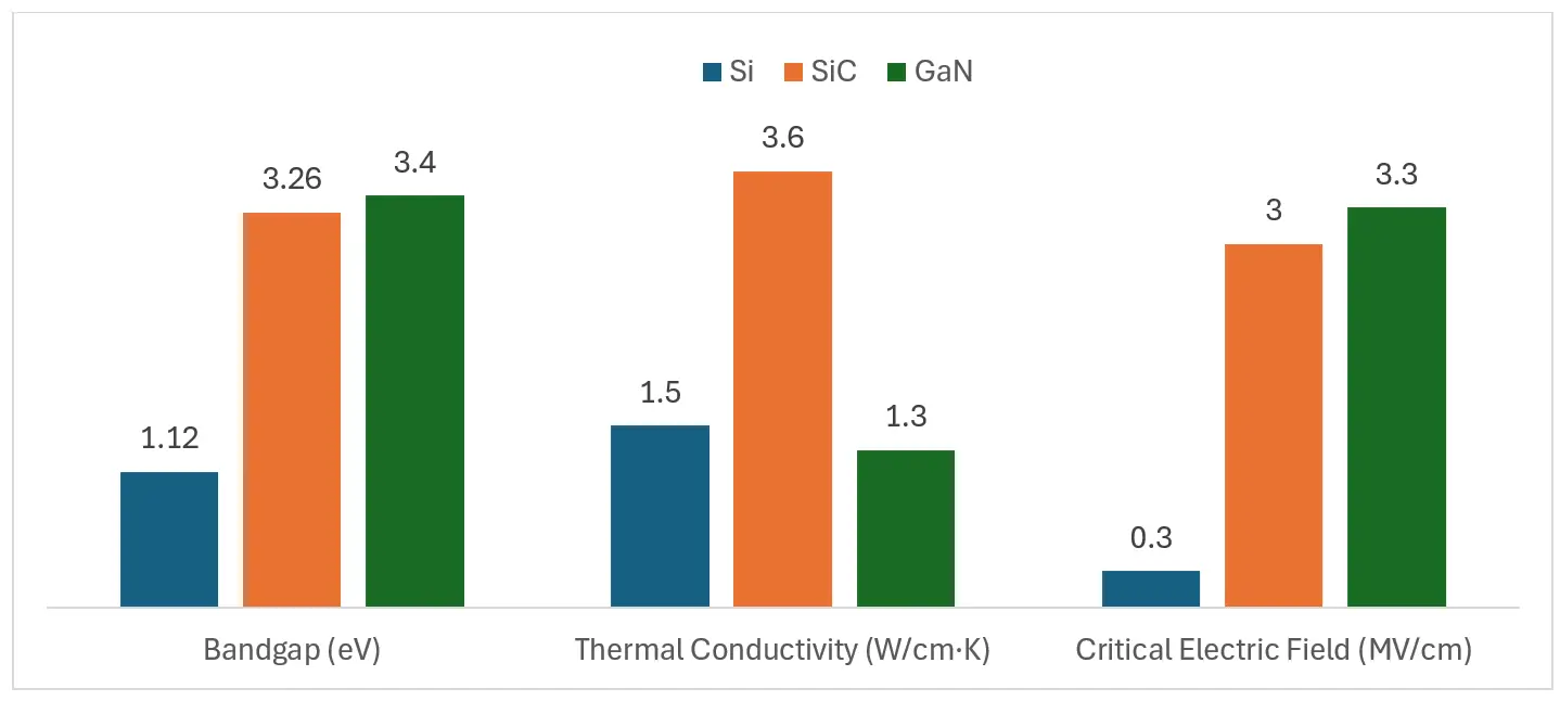
The comparative graph illustrated in Figure 1 shows three critical material properties—thermal conductivity, critical breakdown voltage, and bandgap energy—for Silicon (Si), Silicon Carbide (SiC), and Gallium Nitride (GaN) [14,15]. SiC demonstrates the highest thermal conductivity at 3.6 W/cm·K, enabling superior heat dissipation in high-power applications, whereas Si and GaN exhibit lower values of 1.5 W/cm·K and 1.3 W/cm·K, respectively. In terms of critical electric field, GaN leads with 3.3 MV/cm, followed closely by SiC at 3 MV/cm, indicating their suitability for high-voltage and high-efficiency power electronics, while Si remains limited at 0.3 MV/cm. Regarding bandgap energy, GaN and SiC possess wide bandgaps of 3.4 eV and 3.2 eV, respectively, making them ideal for high-frequency and high-temperature environments, whereas Si’s narrow bandgap of 1.1 eV confines its application to low-power, low-frequency devices. These distinctions underscore the material-dependent nature of semiconductor applications, with Si dominating conventional electronics, SiC excelling in power conversion, and GaN leading in RF and high-speed systems.
Silicon Carbide (SiC) and Gallium Nitride (GaN) represent two leading wide bandgap semiconductor technologies, each optimized for distinct application domains [16,17,18]. SiC power devices employ a vertical structure that supports voltages beyond 900 V, making them ideal for high-power applications such as electric vehicle inverters and industrial motor drives. In contrast, GaN devices use a lateral structure, limiting their voltage capability to approximately 650 V, but enabling superior circuit integration through CMOS-compatible processes. This integration advantage allows GaN to combine power and analog functions, reducing system complexity and footprint.
From a performance perspective, due to high electron mobility and low gate charge, GaN HEMTs excel in high-frequency operation, achieving switching speeds between 200 kHz and 2 MHz—significantly higher than SiC’s 100–300 kHz range. This capability enables smaller passive components and improved efficiency in compact designs. However, SiC outperforms GaN in thermal management, with a thermal conductivity of 3.6 W/cm·K compared to GaN’s 1.3 W/cm·K, ensuring reliability under high-power and high-temperature conditions. Consequently, SiC dominates in high-voltage, high-power systems, while GaN is preferred for low- to mid-voltage applications requiring high efficiency and fast switching. Ultimately, the choice between SiC and GaN depends on application-specific requirements—SiC for robust, high-power environments and GaN for compact, high-frequency designs. The major key differences between SiC and GaN are listed in Table 1.
Table 1. The comparison between GaN and SiC semiconductor devices.
|
GaN |
SiC |
|
|---|---|---|
|
Device Structure |
Lateral |
Vertical |
|
Voltage |
~up to 650 V |
Beyond 900 V |
|
Circuit Integration |
Yes (Power + Analog) |
No |
|
Switching Frequency |
Highest (200 kHz–2 MHz) |
Medium (100–300 kHz) |
|
Thermal Performance |
Same as Silicon (1.3 W/cm·K) |
Highest (3.6 W/cm·K) |
|
Application |
High frequency Low- to mid-voltage |
High power and high thermal performance |
2.2. Bonding Configuration
The SiC JFET cascode configuration, which operates seamlessly with gate drivers designed for standard Si low-voltage MOSFETs (LVMOS), combines the inherent advantages of SiC technology while mitigating the traditional limitations of JFET devices. By leveraging this hybrid structure, the cascode achieves superior static and switching characteristics and enhanced efficiency performance, making it highly suitable for high-power and high-frequency applications [19,20,21]. This approach not only simplifies gate-drive requirements but also ensures robust operation under demanding requirements, positioning SiC JFET cascode as a competitive solution in advanced power electronics. The diagram shown in Figure 2 describes a Cascode configuration consisting of a JFET (top) and a MOSFET (bottom) connected in series. In this structure, the MOSFET acts as the control device, providing easy gate drive compatibility with standard low-voltage signals, while the JFET handles the high-voltage operation. This combination leverages the advantages of both devices: the high-voltage capability and low conduction loss of the JFET, and the simple gate control of the MOSFET
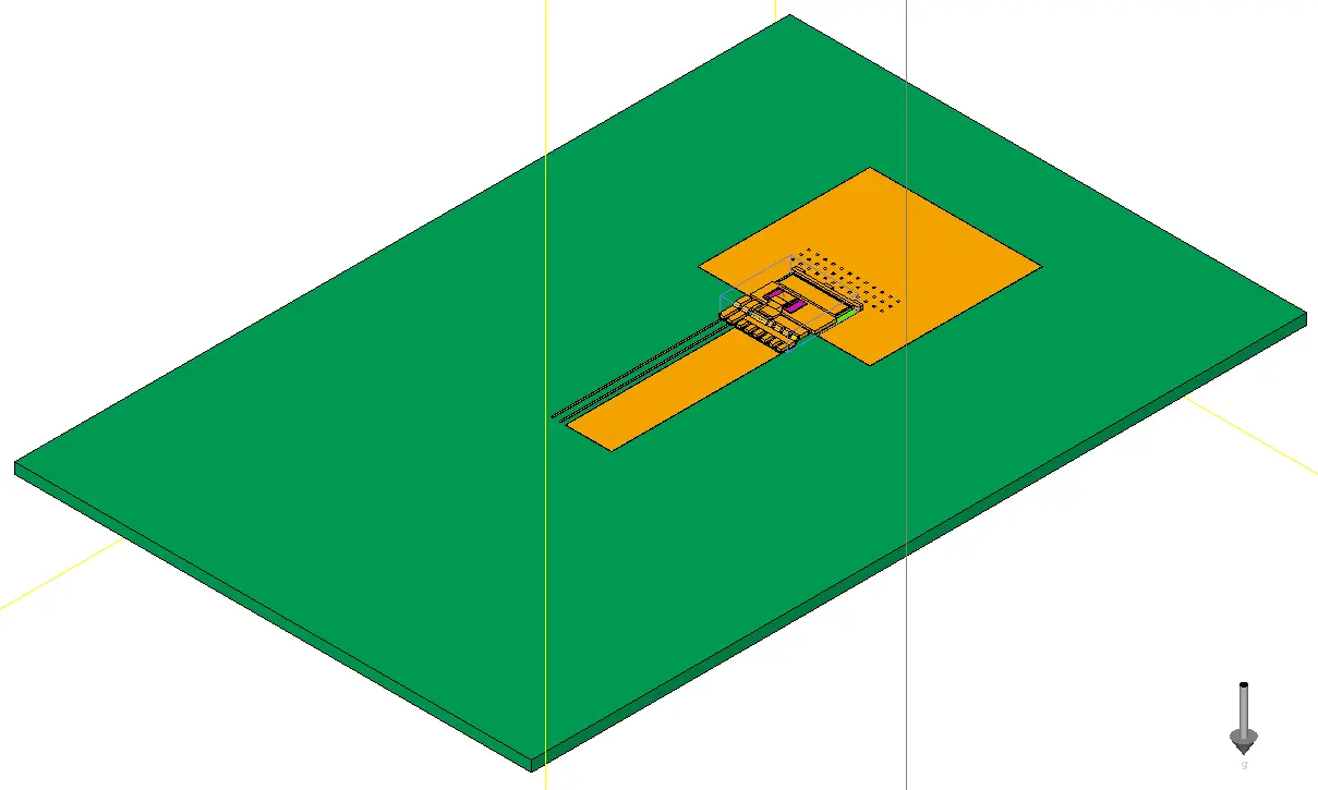
Figure 3 shows a cross-sectional view of a molded package integrating a Silicon MOSFET (Si MOSFET) and a Silicon Carbide (SiC) device in a side-by-side configuration. The Si MOSFET is mounted on a Direct Bonded Copper (DBC) substrate with copper layers to provide superior thermal conductivity and electrical isolation from the high drain voltage. The SiC device is directly attached to the Leadframe for optimized thermal performance. Aluminum wire bonds establish electrical connections, and the entire assembly is encapsulated in a mold compound for mechanical protection and environmental reliability. The Leadframe serves as both structural support and the external electrical interface.

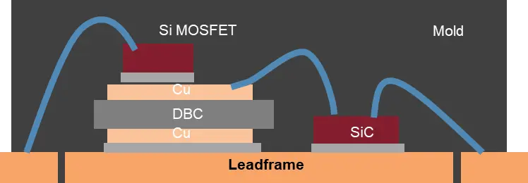
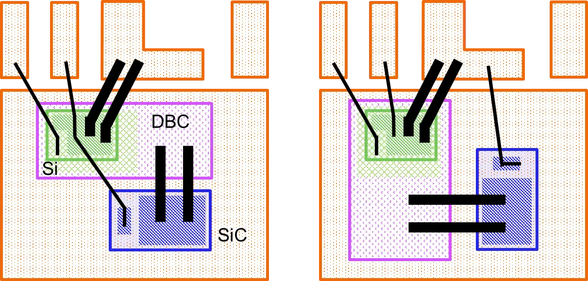
Figure 4 illustrates two alternative bonding configurations for implementing a cascode connection between a Silicon Carbide (SiC) device and a Silicon MOSFET (Si MOSFET). In both cases, the cascode structure is formed by connecting the source of the SiC device to the drain of the Si MOSFET. However, the configurations differ in the method used to bond the SiC gate wire to the Si MOSFET.
-
-
Direct Bonding: In this approach, the gate wire of the SiC device is bonded directly to the source paddle on the Leadframe. This configuration minimizes parasitic inductance and simplifies the interconnection layout.
-
-
Indirect Bonding: In this alternative, the gate wire of the SiC device is bonded to the source of the Si MOSFET, typically combined with a Kelvin source wire connected to the corresponding terminal of the device. This method provides improved gate control and reduces the influence of source stray inductance on switching performance.
These bonding options offer trade-offs between electrical performance and layout complexity, which should be considered during module design. Detailed performance will be discussed in the next section.
 |
|
|
(a) |
(b) |
Figure 4. Two alternative bonding configurations of Cascode device: (a) Indirect bonding option, (b) direct bonding option. The leadframe (orange), Si die (green), SiC die (blue), DCB substrate (purple), and bonding wire (black) are indicated by different colors.
Two different bonding schemes make the difference not only in wire bonding configurations but also in the maximum chip size that can be accommodated within the largest Direct Bonded Copper (DBC) substrate in the package. Consequently, these differences directly affect performance, electrical characteristics, and overall system reliability, making the choice of bonding scheme a critical design decision for high-efficiency and high-power applications.
2.3. Thermal Simulation
In high-power semiconductor applications, the choice of interconnection material significantly affects thermal performance, electrical reliability, and mechanical robustness. Aluminum (Al) wire is widely used for wire bonding due to its cost-effectiveness and good electrical conductivity; however, it faces notable challenges. When implementing Al wire bonding in power modules, a critical issue arises when the SiC die size is smaller than a silicon (Si) die designed for the same power capacity. The reduced footprint of SiC devices, despite their superior thermal and electrical properties, limits the available bonding area, making it difficult to accommodate multiple Al wires for adequate current distribution and mechanical stability. This constraint can lead to increased current density per wire, higher thermal stress, and potential degradation under power cycling. Consequently, alternative interconnection technologies such as CuCorAl composite wire (combining a copper core with aluminum cladding) or clip bonding are increasingly considered to ensure robust performance in high-power SiC-based products.
For die attach, high-lead (High Pb) solder has traditionally been employed due to its high melting point and strong mechanical properties; however, environmental regulations and reliability concerns have driven the industry toward alternative solutions. Sintered silver (Ag) has emerged as a superior option, offering excellent thermal conductivity, low electrical resistance, and enhanced reliability under extreme operating conditions [22,23]. Compared to high-lead solder, sintered Ag provides better heat dissipation and longer lifetime, making it ideal for next-generation high-efficiency and high-power applications. Numerous studies have investigated these materials, particularly in Cascode configurations, where several options for both die attach and DBC attach—illustrated in Figure 3—utilize sintered Ag and high-Pb solder. The thermal performance differences between these approaches have been analyzed through detailed thermal simulations. The package was selected as TOLL with conventional materials but using high-Pb and sintered Ag for die and DBC attachment. The adhesive thickness of the die and DBC over the leadframe is a key contributor to thermal resistance. For this simulation, a 25 µm bond-line thickness was assumed to reflect production control conditions. The material properties used for this simulation are listed in Table 2.
Table 2. The material properties.
|
Class |
Material |
Thermal Conductivity |
Density |
Specific Heat Capacity |
|---|---|---|---|---|
|
(W/m·K) |
(kg/m3) |
(J/kg-K) |
||
|
EMC |
- |
1 |
1850 |
1000 |
|
Die adhesive |
High Pb solder |
25 |
11,010 |
136 |
|
Ag Sinter Paste |
175 |
4000 |
240 |
|
|
Lead Frame/Clip |
C19210 |
364.5 |
8940 |
385.2 |
|
Chip |
SiC |
360 |
3210 |
690 |
|
Si |
117.5 W/m·K at 100 °C Temp. Co. −0.42 W/m·K2 |
2330 |
711 |
|
|
Al-Wire |
Al |
201 |
2700 |
201 |
|
DBC |
Substrate |
25 W/m·K at 25 °C Temp. Co. −0.06 W/m·K2 |
3800 |
880 |
|
Cu |
385 |
8940 |
385.2 |
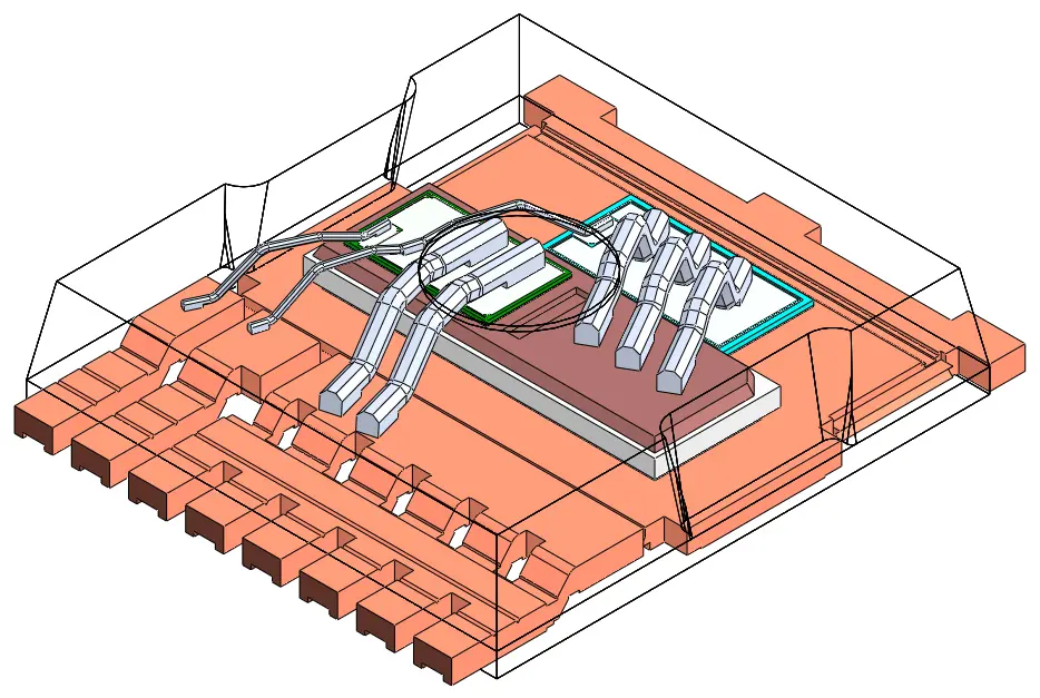
The thermal simulation for Rthja under natural convection was performed using a three-dimensional, steady-state thermal model in Simcenter Flotherm 2304. The analysis incorporated flow, heat transfer, and radiation, with an ambient temperature of 25 °C, in accordance with JEDEC standards 51-3 and 51-7 [24]. The test board consisted of a 1 inch2 copper area with 2 oz copper thickness, PCB dimensions of 76.2 mm × 114.3 mm × 1.6 mm, and SAC305 solder (50 µm). Thermal resistance (Rthja) was evaluated for SiC JFET and Si MOSFET at both chip and package levels using the expression (Tj − Ta)/Pd. Power dissipation was set to 2.8 W for JFET and 0.299 W for MOSFET, maintaining a balance in the required power between SiC JFET and Si MOSFET. The chip dimensions were 3.25 mm2, thickness 0.076 mm for the Si MOSFET and 7.7 mm2, thickness 0.1 mm for the SiC JFET. In the case of Rthjc, the case temperature (T_case) was set to 100 °C, referring to Mil-STD 883-1012 test method [25]. Figure 5a shows a schematic view of the TOLL package, illustrating the wire-bonding configuration between the JFET and LVMOS dies mounted on the DBC, while Figure 5b depicts the corresponding simulation board layout used in the thermal model.
 |
 |
|
(a) |
(b) |
Figure 5. Package and Board Configuration for Thermal Simulation: (a) Schematic view of TOLL package, (b) Simulation board layout.
2.4. System Level Test
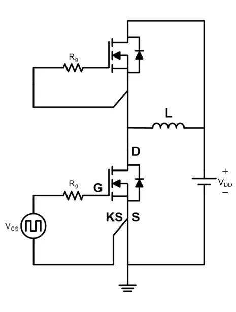
Dynamic performance evaluation of the cascode was performed using the Double Pulse Test (DPT). This included low-line input voltage at maximum output power, full-rated DC bus voltage, and representative thermal load. The test circuit employed a high-speed gate driver with adjustable gate resistance (RG = 1–50 Ω) and bipolar gate voltage levels (+20 V turn-on and −10 V turn-off). Waveforms were captured using a digital oscilloscope with 1-GHz bandwidth and a minimum sampling rate of 5 GS/s. A passive probe was used on the low side, a differential voltage probe on the high-side, and a current probe with a bandwidth greater than 100 MHz to ensure accurate transient characterization. The setup incorporated a low-inductance bus structure and a Kelvin source connection to minimize parasitic effects.
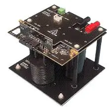
Key parameters recorded included drain-source voltage (VDS) peak, gate-source voltage (VGS) oscillation, switching energy losses (Eon, Eoff), and transient overshoot. In general, this test evaluates switching performance (turn-on/-off) of the device. DPT is not exactly a system-level evaluation, and even if the results meet customer requirements (e.g., 80% of BVDSS), there is no guarantee that the same conditions will be satisfied in the actual customer system. However, DPT is very useful for relative comparison and benchmarking across products. For example, if one device shows a lower VDS peak compared to others, it indicates a performance advantage. Figure 6 shows the DPT test circuit diagram and actual configuration.
 |
 |
|
(a) |
(b) |
Figure 6. The Double Pulse Test (DPT) view: (a) Circuit diagram of the DPC; (b) Actual configuration of the DPC circuit. VGS denotes the gate-to-source voltage, Rg the gate resistor, L the load inductor, VDD the drain supply voltage, and G, D, S, and KS represent the gate, drain, source, and Kelvin source terminals, respectively.
3. Results and Discussion
3.1. Electrical Performance
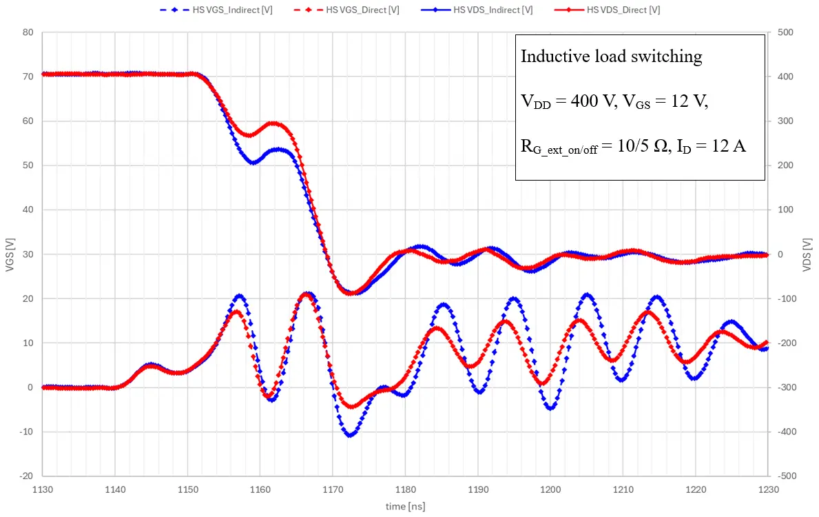
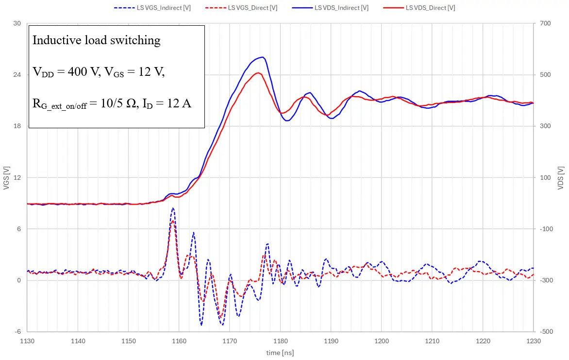
Figure 7 compares the low-side gate-source voltage (VGS) and drain-source voltage (VDS) profiles during the Double Pulse Test (DPT) for direct bonding and indirect bonding configurations. The direct bonding option (red curve) shows a slower low-side VDS dv/dt and approximately 60 V lower VDS overshoot compared to the indirect bonding option (blue curve). This indicates that a larger margin can be secured with respect to derating limits in the customer’s system. In addition, the low-side VGS of the indirect bonding configuration is about 8.5 V, which is approximately 2 V higher than the 6.6 V observed in direct bonding. This demonstrates that the indirect bonding configuration has a higher likelihood of false turn-on of the low-side during the high-side turn-on interval. Both configurations exhibit an oscillation frequency of approximately 40 MHz; however, damping is more effective in the direct bonding case, reducing ringing duration by about 20 ns. During the oscillation phase, the negative peak of the high-side VGS is approximately −10.7 V for indirect bonding, compared to −4.4 V for direct bonding, indicating a deeper peak.
These quantitative differences confirm that direct bonding improves stability by reducing VDS overshoot and VGS bounce due to due to increased stray inductance inside the package. Furthermore, the reduction of VDS overshoot by about 11% and VGS bounce by about 2 V suggests a significant improvement in switching robustness. Lower dv/dt and shorter ringing duration help mitigate EMI concerns and reduce stress on the device during high-speed transitions. As a trade-off, direct bonding shows an increase in switching loss of approximately 7.5%, with an energy loss of 97.8 µJ compared with 90.5 µJ for indirect bonding under a load current of 12 A. In contrast, indirect bonding, while faster due to the absence of additional stray inductance compared to direct bonding, introduces higher dv/dt and an increased likelihood of false turn-on, which may potentially impact long-term reliability and thermal performance. Therefore, direct bonding is recommended for applications requiring high switching speed and strict EMI compliance. Key Metrics for Direct vs. Indirect Bonding under DPT Conditions are compared in Table 3.
 |
|
(a) |
 |
|
(b) |
Figure 7. Comparison of gate-source voltage (VGS) and drain-source voltage (VDS) waveforms during Double Pulse Test for direct bonding (red) and indirect bonding (blue) configurations. Direct bonding exhibits reduced low-side VDS overshoot (506 V vs. 568 V) and lower low-side Gate bounce (6.6 V vs. 8.5 V), indicating improved switching stability and increased parasitic inductance compared to indirect bonding. (a) Waveforms of high-side, (b) Waveforms of low-side when high-side turns on. The specific test conditions are indicated within the figure.
Table 3. Comparison of Key Metrics for Direct vs. Indirect Bonding under DPT Conditions.
|
Parameter |
Direct Bonding |
Indirect Bonding |
|---|---|---|
|
Peak VDS Overshoot |
506 V |
568 V |
|
Gate Oscillation Amplitude |
6.6 V |
8.5 V |
|
Oscillation Frequency |
~40 MHz |
~40 MHz |
|
Ringing Duration |
~50 ns |
~70 ns |
|
Negative Current Peak |
−4.4 V |
−10.7 V |
The differences observed in the Double Pulse Test (DPT) results between direct and indirect bonding configurations can be explained by the current flow paths shown in Figure 8. In the direct bonding configuration (red path), the connection from the JFET gate to the Kelvin source introduces additional inductance, resulting in a higher overall path inductance of 8.8 nH compared with 6.2 nH for the indirect bonding configuration (blue path). This increase in inductance reduces VDS voltage overshoot and mitigates VGS oscillation, as confirmed by approximately 60 V lower low-side VDS overshooting during the low-side turn-off transition and 2 V lower low-side VGS bounce during the high-side turn-on transition. Although the overall inductance is higher, it slows down dv/dt and reduces peaking, resulting in faster damping of oscillations and improved switching stability.
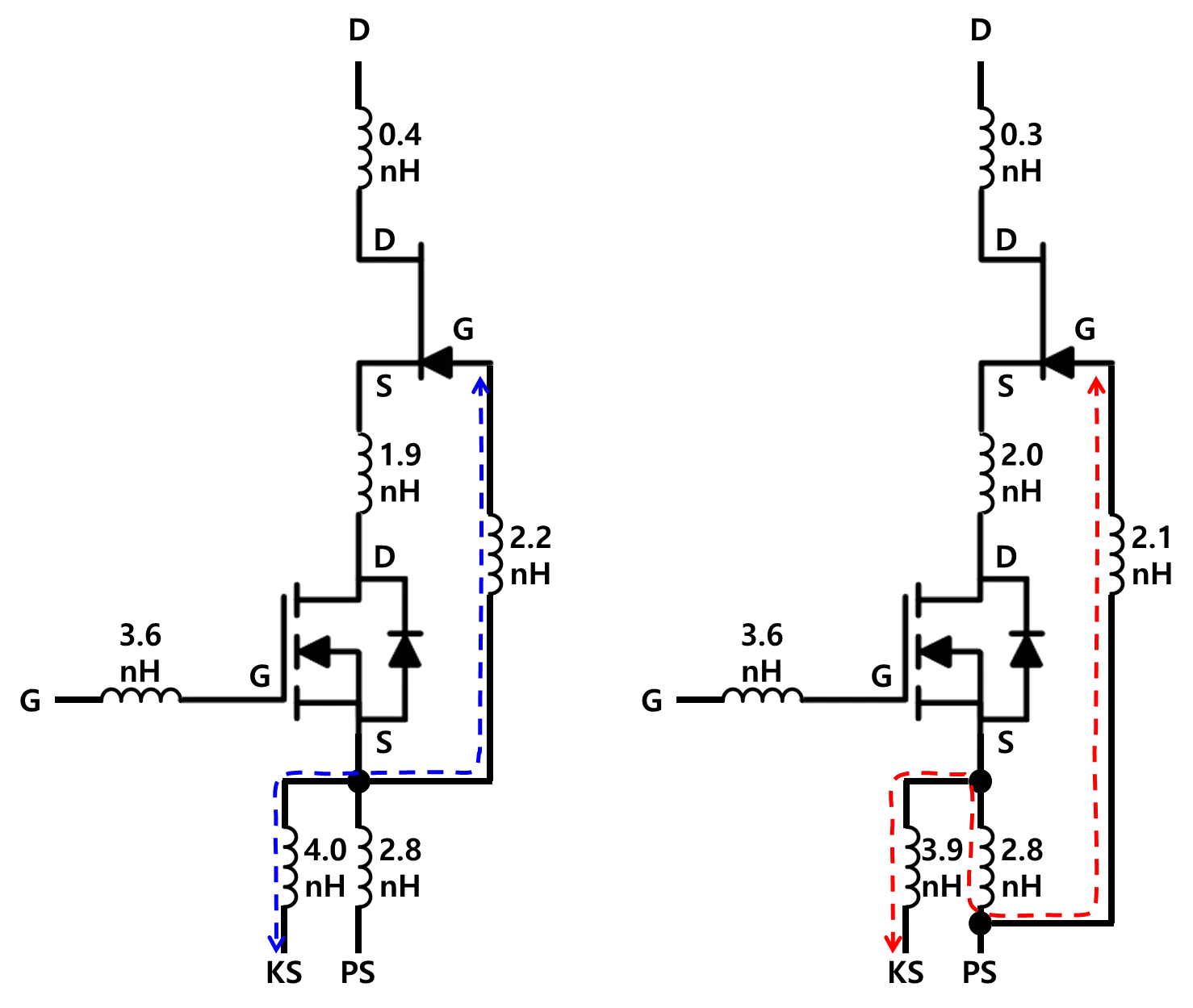
Figure 8. Current flow paths for direct bonding (red dashed line) and indirect bonding (blue dashed line) in the Double Pulse Test circuit. Direct bonding provides a longer return path to the Kelvin source, increasing loop inductance and associated parasitic effects, while indirect bonding introduces a shorter path with lower inductance, increasing voltage overshoot and gate oscillation during switching events. G, D, S, PS, and KS represent the gate, drain, source, power source, and Kelvin source terminals, respectively.
Conversely, the indirect bonding option (blue path) connects the JFET Gate directly to the Kelvin source, reducing the overall inductance. This lower inductance causes higher VDS overshoot and larger gate oscillations. The increased ringing duration and the negative peak of the high-side VGS observed in the waveform further indicate that indirect bonding exacerbates dynamic stress during turn-off events. These effects can lead to higher EMI emissions and potential reliability concerns under high-speed switching conditions.
Overall, the analysis shows that while direct bonding increases parasitic inductance inside the package, it ultimately improves dynamic behavior and provides superior electrical performance, making it the preferred choice for applications requiring high efficiency and robust switching characteristics.
3.2. Thermal Performance
Table 4 summarizes the simulation conditions for thermal analysis, where different die attach materials are applied to each component in a SiC JFET-based structure. Three configurations are considered: Option 1 uses High-Pb solder for all components (Si MOSFET, DBC, and SiC); Option 2 applies High-Pb solder to Si MOSFET and DBC while using Sintered Ag for SiC; and Option 3 employs Sintered Ag for all components.
Table 4. Simulation configurations for thermal analysis of SiC JFET-based power module.
|
Option 1 |
Option 2 |
Option 3 |
|
|---|---|---|---|
|
Si MOSFET |
High Pb solder |
High Pb solder |
Sinter Ag |
|
DBC |
High Pb solder |
High Pb solder |
Sinter Ag |
|
SiC |
High Pb solder |
Sinter Ag |
Sinter Ag |
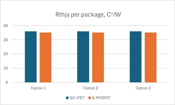
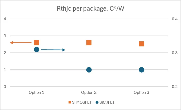
The thermal simulation results, illustrated in Figure 9, compare the junction-to-ambient thermal resistance (Rthja per package) and junction-to-case thermal resistance (Rthjc per package) for SiC JFET and Si MOSFET devices under three different attach material configurations. Si MOSFET exhibits slightly lower Rthja values at approximately 35 °C/W compared to SiC JFET at around 36 °C/W. This suggests that changes in attach material have minimal impact on overall heat dissipation to the ambient environment, as this path is primarily governed by package design with insulated substrate, power dissipation balance of devices, and system-level cooling.
In contrast, Rthjc reveals more significant trends. Si MOSFET consistently shows higher Rthjc values (around 2.5 °C/W) compared to SiC JFET (approximately 0.3 °C/W), indicating that intrinsic device structure dominates junction-to-case heat transfer. However, for SiC JFET, the use of sintered Ag in Options 2 and 3 reduces Rthjc by roughly 20% compared to High-Pb solder, which is a substantial improvement. This demonstrates that advanced attach materials can meaningfully enhance heat dissipation at the die-to-case interface for wide-bandgap devices like SiC, where thermal management is critical for reliability and performance. In contrast, Si MOSFET shows negligible benefit, reinforcing that material impact is highly device and package dependent.
Overall, these results highlight that while sintered Ag offers clear advantages for SiC devices, its influence on Si MOSFET thermal resistance remains limited. Future optimization should combine advanced attach materials with improved package architecture and heat spreading strategies to fully leverage the benefits of high-conductivity materials.
 |
 |
|
(a) |
(b) |
Figure 9. Thermal resistance comparison for SiC JFET and Si MOSFET under three attach material configurations: (a) Junction-to-ambient thermal resistance (Rthja); (b) Junction-to-case thermal resistance (Rthjc). The left-pointing orange arrow represents the left y‑axis, while the right-pointing blue arrow represents the right y‑axis.
4. Conclusions
The Double Pulse Test (DPT) results, analyzed alongside the current flow paths, clearly demonstrate the significant impact of bonding configuration on the dynamic performance of cascode devices. This work establishes that direct bonding, despite introducing higher parasitic inductance within the JFET’s gate path, effectively reduces VDS overshoot and mitigates VGS oscillations under high-speed switching conditions. As a result, slower dv/dt, faster damping of oscillations, and improved switching stability are achieved, as confirmed by approximately 60 V lower VDS overshoot and 2 V lower VGS bounce during critical transitions. In contrast to the conventional approach that prioritizes inductance minimization, the indirect bonding configuration is shown to increase voltage overshoot, prolong ringing, and intensify gate oscillations, leading to higher dynamic stress and potential reliability concerns. These findings underscore the importance of interconnect design in achieving robust, high efficiency operation for wide bandgap devices under system level stress conditions.
In parallel, the thermal analysis conducted in this work clarifies the distinct roles of system level cooling and die attach material selection. While external cooling conditions primarily govern Rthja, this study demonstrates that the use of sintered Ag die attach yields an approximately 20% reduction in Rthjc for SiC JFET devices compared to conventional High Pb solder. This improvement translates into higher current ratings, lower junction temperatures, extended device lifetime, and enhanced reliability for SiC based applications. Therefore, sintered Ag not only strengthens mechanical integrity but also delivers measurable thermal benefits, reinforcing its value in optimizing performance and durability for wide bandgap devices.
Statement of the Use of Generative AI and AI-Assisted Technologies in the Writing Process
During the preparation of this manuscript, the authors used [M/S Copilot] in order to [refine the sentence overall]. After using this service, the authors reviewed and edited the content as needed and take full responsibility for the content of the published article.
Author Contributions
Conceptualization, B.K.; Methodology, B.K., C.K. and B.L.; Validation, B.K., C.K., B.L. and A.B.; Formal Analysis, C.K. and B.L.; Investigation, B.K., C.K., B.L. and A.B.; Writing—Original Draft Preparation, B.K.; Writing—Review & Editing, B.K., C.K., B.L. and A.B.; Visualization, B.K.; Supervision, B.K. and A.B.; Project Administration, B.K. and A.B.
Ethics Statement
Not applicable.
Informed Consent Statement
Not applicable.
Data Availability Statement
The data supporting the findings of this study are available upon reasonable request.
Funding
This research received no external funding.
Declaration of Competing Interest
The authors declare that they have no known competing financial interests or personal relationships that could have appeared to influence the work reported in this paper.
References
- Rabkowski J, Peftitsis D, Nee H-P. Silicon Carbide Power Transistors: A New Era in Power Electronics Is Initiated. IEEE Ind. Electron. Mag. 2012, 6, 17–26. DOI:10.1109/MIE.2012.2193291 [Google Scholar]
- Millán J, Godignon P, Perpiñà X, Pérez-Tomás A, Rebollo J. A Survey of Wide Bandgap Power Semiconductor Devices. IEEE Trans. Power Electron. 2014, 29, 2155–2163. DOI:10.1109/TPEL.2013.2268900 [Google Scholar]
- Cooper JA, Melloch MR, Singh R, Agarwal A, Palmour JW. Status and prospects for SiC power MOSFETs. IEEE Trans. Electron Devices 2002, 49, 658–664. DOI:10.1109/16.992876 [Google Scholar]
- Bolotnikov A, Losee P, Permuy A, Dunne G, Kennerly S, Rowden B, et al. Overview of 1.2kV–2.2kV SiC MOSFETs targeted for industrial power conversion applications. In Proceedings of the 2015 IEEE Applied Power Electronics Conference and Exposition (APEC), Charlotte, NC, USA, 15–19 March 2015; pp. 2445–2452. DOI:10.1109/APEC.2015.7104691 [Google Scholar]
- Chiu PK, Lin HH, Huan YC, Syu JY, Liu YC, Fan YB, et al. The Development of 1.7kV 100A SiC MOSFET Power Module for Automotive Application. In Proceedings of the 2023 IEEE Workshop on Wide Bandgap Power Devices and Applications in Asia (WiPDA Asia), Hsinchu, Taiwan, 27–29 August 2023; pp. 1–4. DOI:10.1109/WiPDAAsia58218.2023.10261934 [Google Scholar]
- Mysinski W. SiC mosfet transistors in power analog application. In Proceedings of the 2017 19th European Conference on Power Electronics and Applications (EPE’17 ECCE Europe), Warsaw, Poland, 11–14 September 2017; pp. P.1–P.7. DOI:10.23919/EPE17ECCEEurope.2017.8099305 [Google Scholar]
- Ramachandran R, Nymand M, Østergaard C, Kjeldsen C, Kapino G. High efficiency 20kW SiC based Isolated DC-DC Converter for Battery Charger Applications. In Proceedings of the 2018 20th European Conference on Power Electronics and Applications (EPE’18 ECCE Europe), Riga, Latvia, 17–21 September 2018; pp. P.1–P.9. [Google Scholar]
- Alexandrov P, Bhalla A, Li ZD, Li XQ, Bendel J, Dodge J. 650V SiC cascode: A breakthrough for wide-bandgap switches. In Proceedings of the 2016 European Conference on Silicon Carbide & Related Materials (ECSCRM), Halkidiki, Greece, 25–29 September 2016; pp. 673–676. DOI:10.4028/www.scientific.net/MSF.897.673 [Google Scholar]
- Treu M, Rupp R, Blaschitz P, Ruschenschmidt K, Sekinger T, Friedrichs P, et al. Strategic Considerations for Unipolar SiC Switch Options: JFET vs. MOSFET. In Proceedings of the 2007 IEEE Industry Applications Annual Meeting, New Orleans, LA, USA, 23–27 September 2007; pp. 324–330. [Google Scholar]
- Cascode Primer. Application Note: AND90328/D. Operation of the SiC Cascode JFET. 2025. Available online: https://www.onsemi.com/download/application-notes/pdf/and90328-d.pdf (accessed on 15 January 2026).
- Kim B, Bolotnikov A, Jeong H, Kim C, Das H, Ponram G. Advanced SiC Power Technology and Package. In Proceedings of the 2023 7th IEEE Electron Devices Technology & Manufacturing Conference (EDTM), Seoul, Republic of Korea, 7–10 March 2023; pp. 1–3. DOI:10.1109/EDTM55494.2023.10103126 [Google Scholar]
- Schuderer J, Vemulapati U, Traub F. Packaging SiC power semiconductors—Challenges, technologies and strategies. In Proceedings of the 2014 IEEE Workshop on Wide Bandgap Power Devices and Applications, Knoxville, TN, USA, 13–15 October 2014; pp. 18–23. DOI:10.1109/WiPDA.2014.6964616 [Google Scholar]
- Grummel B, McClure R, Lei Zhou, Gordon AP, Chow L, Shen ZJ. Design consideration of high temperature SiC power modules. In Proceedings of the 2008 34th Annual Conference of IEEE Industrial Electronics, Orlando, FL, USA, 10–13 November 2008; pp. 2861–2866. DOI:10.1109/IECON.2008.4758413 [Google Scholar]
- Woo K, Bian Z, Noshin M, Perez Martinez R, Malakoutian M, Shankar B, et al. From wide to ultrawide-bandgap semiconductors for high power and high frequency electronic devices. J. Phys. Mater. 2024, 7, 022003. DOI:10.1088/2515-7639/AD218B [Google Scholar]
- Yuvaraja S, Khandelwal V, Tang X, Li X. Wide bandgap semiconductor-based integrated circuits. Chip 2023, 2, 100072. DOI:10.1016/J.CHIP.2023.100072 [Google Scholar]
- Bogdanovs A, Krievs O, Pforr J. Wide Bandgap SiC and GaN Semiconductor Performance Evaluation in a 3-Phase 3-Level NPC Inverter for Transportation Application. In Proceedings of the 2022 IEEE 63th International Scientific Conference on Power and Electrical Engineering of Riga Technical University (RTUCON), Riga, Latvia, 10–12 October 2022; pp. 1–7. DOI:10.1109/RTUCON56726.2022.9978767 [Google Scholar]
- Zhang Z, Wang F, Tolbert LM, Blalock BJ, Costinett D. Understanding the limitations and impact factors of wide bandgap devices’ high switching-speed capability in a voltage source converter. In Proceedings of the 2014 IEEE Workshop on Wide Bandgap Power Devices and Applications, Knoxville, TN, USA, 13–15 October 2014; pp. 7–12. DOI:10.1109/WiPDA.2014.6964614 [Google Scholar]
- Heckman R, Quinn C. The Growth of Wide Bandgap Technology in Industrial Power Conversion. IEEE Power Electron. Mag. 2024, 11, 54–60. DOI:10.1109/MPEL.2024.3492294 [Google Scholar]
- Rodriguez A, Fernandez M, Hernando MM, Lamar DG, Arias M, Sebastian J. Switching performance comparison of the SiC JFET and the SiC JFET/Si MOSFET cascode configuration. In Proceedings of the 2013 IEEE Energy Conversion Congress and Exposition, Denver, CO, USA, 15–19 September 2013; pp. 472–479. DOI:10.1109/ECCE.2013.6646739 [Google Scholar]
- Shu J, Sun J, Tao M, Du Y, Chen T, Lee SWR, et al. 3D Co-packaging of GaN/SiC Cascode Device for High-Frequency Power Switching Operation. In Proceedings of the 2024 36th International Symposium on Power Semiconductor Devices and ICs (ISPSD), Bremen, Germany, 2–6 June 2024; pp. 486–489. DOI:10.1109/ISPSD59661.2024.10579564 [Google Scholar]
- Xie R, Shi Y, Li H. Study of 1200 V SiC JFET cascode device. In Proceedings of the 2017 IEEE 5th Workshop on Wide Bandgap Power Devices and Applications (WiPDA), Albuquerque, NM, USA, 30 October–1 November 2017; pp. 316–320. DOI:10.1109/WiPDA.2017.8170566 [Google Scholar]
- Wang H, Yang D, Cai M, Wang X, Liang Z. Thermal Simulation Modeling of IGBT Module Using Silver Nanoparticle Sintering Material. In Proceedings of the 2018 19th International Conference on Electronic Packaging Technology (ICEPT), Shanghai, China, 8–11 August 2018; pp. 904–907. DOI:10.1109/ICEPT.2018.8480728 [Google Scholar]
- Wakamoto K, Namazu T. Mechanical Characterization of Sintered Silver Materials for Power Device Packaging: A Review. Energies 2024, 17, 4105. DOI:10.3390/en17164105 [Google Scholar]
- JEDEC. Available online: https://www.jedec.org/standards-documents (accessed on 15 January 2026).
- Department of Defense. 1997. Available online: https://nepp.nasa.gov/docuploads/31ECBD46-FFA0-43AE-82C09A3B2B6FE26B/std883.pdf (accessed on 15 January 2026).