Review of Gallium Nitride Devices and Integrated Circuits at High Temperatures

Review of Gallium Nitride Devices and Integrated Circuits at High Temperatures
Kepeng Zhao 1,† Pingyu Cao 1,2,† Jie Jiao 1 Yihao Xu 1 Zhengxuan Li 1 Miao Cui 1,* Fei Xue 1
Received: 30 July 2025 Revised: 20 August 2025 Accepted: 19 September 2025 Published: 29 September 2025

© 2025 The authors. This is an open access article under the Creative Commons Attribution 4.0 International License (https://creativecommons.org/licenses/by/4.0/).
1. Introduction
Integrated circuits play a vital role in diverse industries and serve as the foundation of the modern information society. The majority of commercial integrated circuits are based on silicon devices. However, the performance of silicon devices significantly declines at elevated temperatures, and they may even become damaged when the operating temperature exceeds 125 ℃. Numerous industrial applications require high-temperature capabilities that exceed 125 ℃, even 500 ℃. For instance, turbine engines necessitate the placement of sensors in an ambient temperature of 500 ℃ [1]. Similarly, in aerospace exploration, electronic components are required to withstand extreme radiation environments and ambient temperatures that can surpass 500 ℃ [2]. The application of integrated circuits in numerous scenarios, such as aerospace, will be restricted. Extra cooling systems can mitigate this issue, but it hinder the enhancement of integration and increase the volume and cost of the integrated circuits. Consequently, it is imperative to explore alternative approaches that are more integration-friendly. Wide bandgap semiconductors, such as gallium nitride (GaN) and Silicon carbide (SiC), are considered promising candidates for applications necessitating exposure to elevated temperatures. SiC and GaN are well-established wide bandgap devices known for their attractive features, including high current carrying capabilities, low on-resistances, wide bandgap, high breakdown field and good thermal conductivity [3]. Meanwhile, the combined figure of merit (CFOM) of GaN devices based on various substrates was evaluated, and it was observed that the GaN device utilizing a sapphire substrate exhibited the highest CFOM [3]. Compared to Si-based devices, a proposed GaN vertical superjunction high electron mobility transistor (SJ HEMT) exhibits substantial performance improvement with respect to on-state resistance and breakdown field [4]. Furthermore, HEMTs can show stable DC characteristics after being tested at 400 ℃ for 25 h, which is manifested by negligible changes in characteristics such as saturation current and threshold voltage. Reviews have been published on the relevant characteristics of wide bandgap devices, including the advantages and challenges [5,6,7,8]. Additionally, specific review [9,10] concentrated on furnishing background information about GaN power devices and GaN-based integrated circuits. The existing reviews cover the high-temperature device characteristics of HEMTs and some basic HEMT-based circuits and sensors [11].This review aims to analyze thermal degradation mechanisms and high-temperature applications of GaN HEMTs from a process perspective. The paper lists the manufacturing processes and their high-temperature limits associated with different device structures. It then comprehensively analyzes the results based on theoretical models, simulation data, and experimental results. Subsequently, from an application perspective, this review outlines various GaN integrated circuits and analyzes the performance degradation at high temperatures. Numerous studies have demonstrated that GaN integrated circuits exhibit exceptional thermal stability at temperatures ranging from 200 ℃ to 400 ℃. This review offers valuable insights for small power devices and their integrated circuit applications.
This review presents the performance of GaN devices in Section 2, including the basic principles of GaN devices. This section also examines the high-temperature performance of various GaN devices and explains the effect of temperature on their fundamental properties. In Section 3, the degradation mechanisms under high temperatures are introduced. Moreover, the integrated circuits based on GaN technologies are examined in Section 4. Section 5 summarises our main findings.
2. Gallium Nitride Devices
Previous research indicated that GaN, a wide bandgap semiconductor, is a promising material choice for high-temperature environments. This section will examine GaN devices proposed and applied at high temperatures, including their characteristics and similarities.
GaN HEMTs can be categorised into two types: enhancement mode (E-mode) and depletion mode (D-mode). Different gate process techniques have been implemented in GaN HEMTs, such as metal-insulator-semiconductor (MIS) HEMTs, P-type GaN HEMTs, etc. The effect of temperature on the electrical properties of GaN devices has been reported. GaN devices could operate at a high temperature of up to 600 ℃, indicating their great potential for high temperature applications.
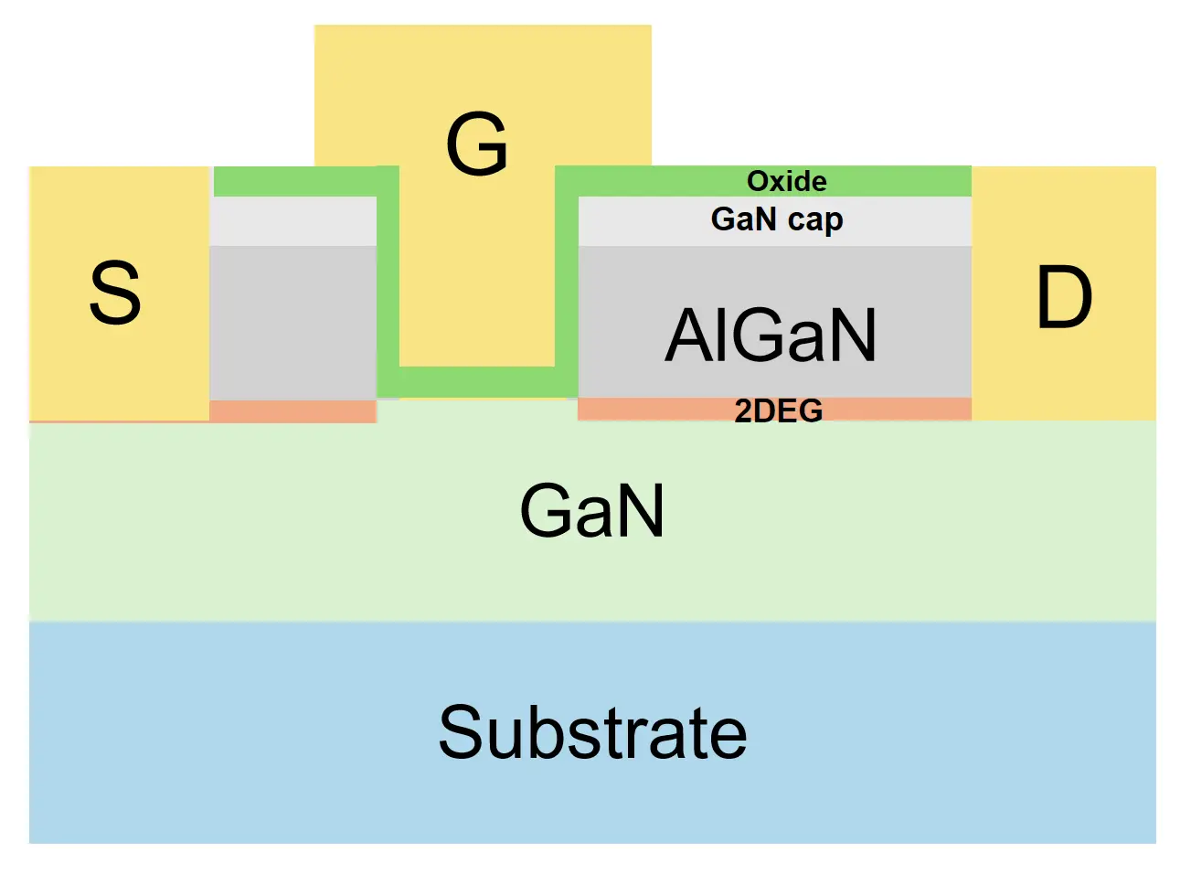
The heterostructure of Aluminium Gallium Nitride (AlGaN) and GaN is proposed to replace Si MOSFETs for high frequency power switching applications. However, the natural channel of this heterojunction makes it a normally-on device. Normally-off AlGaN/GaN HEMTs with positive gate threshold voltage are recommended for power supply applications to ensure safe operation. E-mode devices can be achieved by three technical approaches: p-GaN (or p-AlGaN) cap layers, gate recess, and fluorine plasma processing.
2.1. The HT Characteristics of GaN HEMTs
The performance of GaN devices significantly affects the performance of circuits in power electronics, making the study of device characteristics at different temperatures a valuable area for further research. The manufacturing technology of E-mode GaN HEMTs by fluorine implantation has attracted significant interest [12,13]. The principle of F implantation is to introduce negative fluorine ions in the AlGaN barrier, resulting in the effective depletion of the 2DEG in the channel.
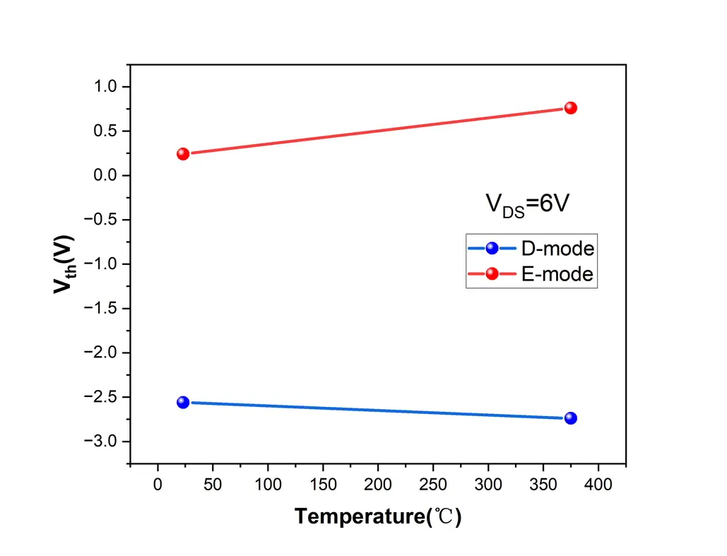
In 2007, a normally-off GaN HEMT with fluorine plasma treatment was fabricated and measured in a temperature range from 25–375 ℃ [12]. The E-mode AlGaN/GaN HEMT has a threshold voltage (Vth) of 0.76 V at 23 ℃, and the drain current at Vgs =3 V is 250 mA/mm, with a peak transconductance of 120 mS/mm. As the measurement temperature increases, threshold voltage, drain current density, and peak transconductance are 0.24 V, 56 mA/mm, and 29 mS/mm at 375 ℃, respectively. As summarized in Figure 1, the D-mode device shows a negative threshold voltage shift of 0.18 V at 375 ℃ compared to the E-mode device. A decrease in current density and peak transconductance was observed as 87 mS/mm, 267 mA/mm at VG = 1 V, respectively.
Based on Fluorine ion treatment, post-gate annealing technology for GaN HEMTs can increase the threshold voltage at room temperature and reduce voltage threshold drift at high temperatures [13]. As temperature increases, the negative shift of the threshold voltage is caused by thermal excitement of electrons which are trapped by Fluoride ions. Consequently, the amount of negatively charged Fluoride ions in the AlGaN layer decreases, resulting in a negative shift of the threshold voltage at high temperatures. The negative temperature coefficient of Vth in Fluorine ion-based HEMTs can be alleviated by a thinner barrier and slightly lower Al compositions, while the increased threshold voltage can be achieved by larger doses of plasma treatment [14].
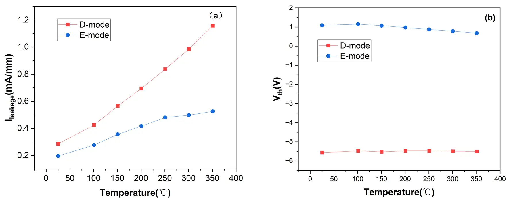
The leakage current of GaN HEMTs increases with rising temperature. However, the increased magnitude of leakage current in E-mode devices is significantly lower than that of D-mode devices, as illustrated in Figure 2. The difference is due to the presence of fluoride ions in the AlGaN layer of HEMTs [15]. The threshold voltage has a small variation across various temperatures. The on-state resistance (Ron) of GaN devices also increases as the temperature rises. The primary causes are high off-state voltage and switching transients at elevated junction temperatures [16].
Studies demonstrate that employing a high-thermal-conductivity substrate, particularly SiC, can reduce the effective thermal resistance by an order of magnitude and significantly enhance the thermal performance of GaN devices. Gaska et al. [17] were the first to fabricate AlGaN/GaN HFETs on a 6H-SiC substrate, achieving a room-temperature dissipated power of 0.6 MW/cm² and stable operation up to 300 ℃, verifying that GaN-on-SiC boosts DC power handling to over three times that of sapphire substrate based devices. Maeda et al. [18] subsequently pushed the operating temperature to 400 ℃ on SiC substrates, with only an 8% drop in transconductance. This demonstrated that the high thermal conductivity substrate effectively suppresses the rise in junction temperature. In 2002, Arulkumaran et al. [19] compared AlGaN/GaN HEMTs and found that device performance on a SiC substrate outperformed that on a sapphire substrate when the temperature is less than 300 ℃. Cuerdo et al. [20] later used source/drain resistance extraction to show that Si (111) devices, owing to higher thermal conductivity, exhibit higher ID and Gm than sapphire at room temperature. However, this difference disappears above 300 ℃, reinforcing SiC’s advantages in the typical operating range. Islam et al. [21] further demonstrated that combining SiC with 140 nm short-gate structures retains 35% of the initial current at 500 ℃, whereas sapphire substrates show faster degradation, underscoring SiC’s superior heat dissipation.
2.2. The HT Characteristics of GaN MIS-HEMTs
GaN devices often incorporate gate insulators under the gate electrode to improve device performance, such as reducing leakage current and increasing gate swing. Alumina (Al2O3) functions as a metal insulator, thereby preventing gate metal sinking at elevated temperatures and reducing leakage current. This effect is evident in the fact that metal insulators can withstand temperatures in excess of 600 ℃ without degradation, whereas HEMTs can only tolerate temperatures up to 300 ℃ before experiencing a sudden increase in leakage current [22]. The DC characteristics at HTs are shown in Figure 3.
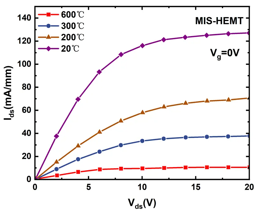
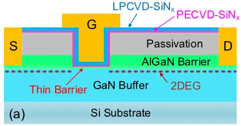
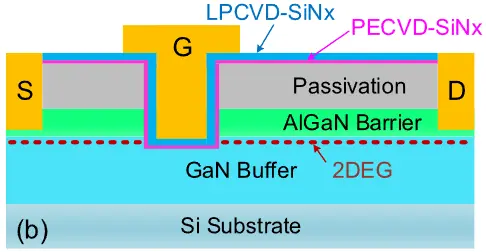
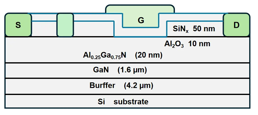
A GaN MIS-HEMT using aluminum oxide as the gate dielectric was measured from 25 ℃ to 600 ℃. The results indicates that the Ron of the MIS-HEMT increased by about eight times [22]. Furthermore, the gate dielectric can be achieved through multilayer fluorinated ALD-Al2O3 layers, which would lead to a high threshold voltage at room temperature, while the threshold voltage presents a slight negative shift under elevated temperatures, which is affected by the thickness of the barrier layer [23,24]. AlGaN barrier recess technology with different etching depths has different impacts on GaN devices shown in Figure 4. GaN MIS-FETs fabricated with fully recessed gate technology can yield a beneficially greater Vth, thus reducing the likelihood of false turn-on events. The Vth of partially recessed MIS-HEMTs and fully recessed MIS-FETs are +0.4 V and +2.37 V at room temperature, respectively. When the temperature reaches 200 ℃, the threshold voltage shift ΔVth is −0.76 V and −0.21 V for the partially and fully recessed devices, respectively. However, on-state resistance is negatively affected by the removal of the heterojunction in Figure 4b, resulting in a relatively high Ron (13.2 Ω·mm). The partially recessed MIS-HEMT in Figure 4a maintains a thin barrier layer, leading to a smaller Ron of 9.6 Ω·mm [25].
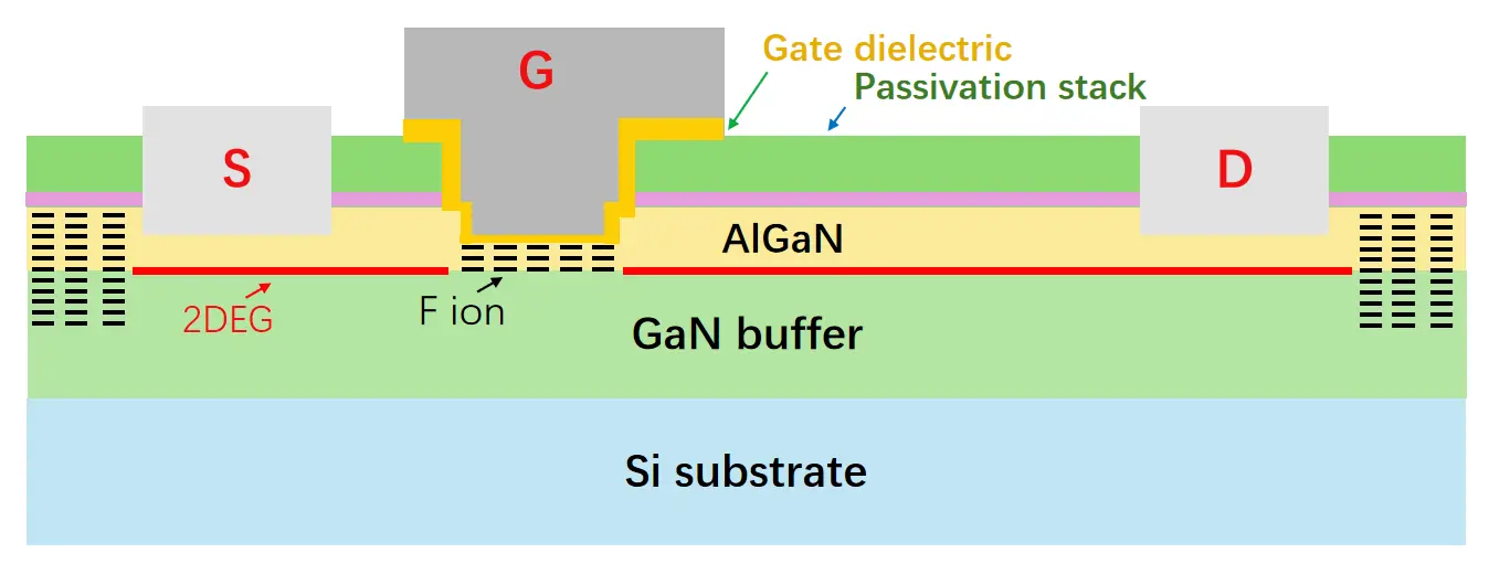
Combined with fluorine plasma implantation and gate recess technology, Liu et al. [26] designed an E-mode MIS-HEMT, as illustrated in Figure 5. This hybrid structure leads to a less negative Vth shift than MIS-HEMTs without gate recess. The device presents a slight negative Vth shift of -0.5V from room temperature to 200 ℃ [26]. The experimental results indicate that the Vth thermal stability of the E-mode device is improved as the barrier thickness is reduced.
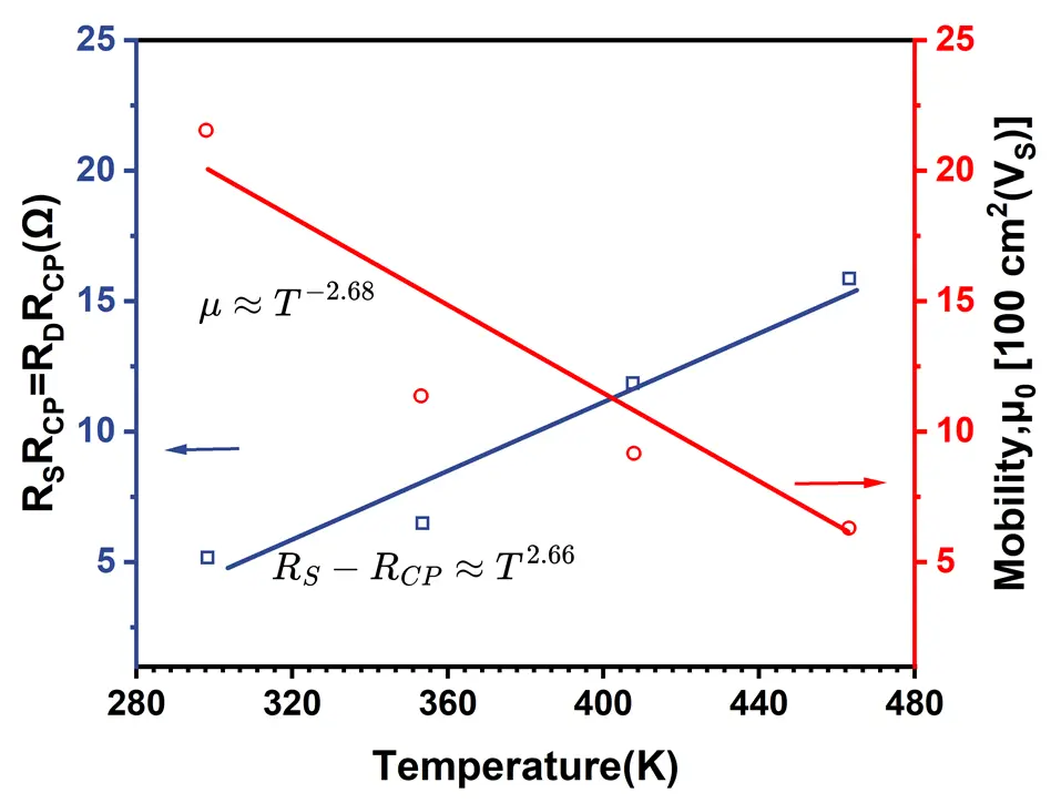
Wang et al. [24] used the charge analytical model and Poole-Frenkel trap emission theory to study the fluorinated trap states distribution of GaN MIS-HEMTs. The positive correlation between the fluorine treatment power and the trap state density is clarified. An improved DC Extraction method [27,28] based on the UFM model proposed by Dasari et al. yields a series of parameters that consider factors such as self-heating effects in GaN HEMTs. In subsequent work [29], they used this method to study the temperature dependence and high-temperature characteristics of low field channel mobility μ0 and parasitic resistances RS/RD. Figure 6 shows the parameters extracted by this model, where mobility μ0 decreases with increasing temperature, while 2DEG resistance increases. All the variations follow a power law ~Tγ (−3.42 < γ < −2.18).
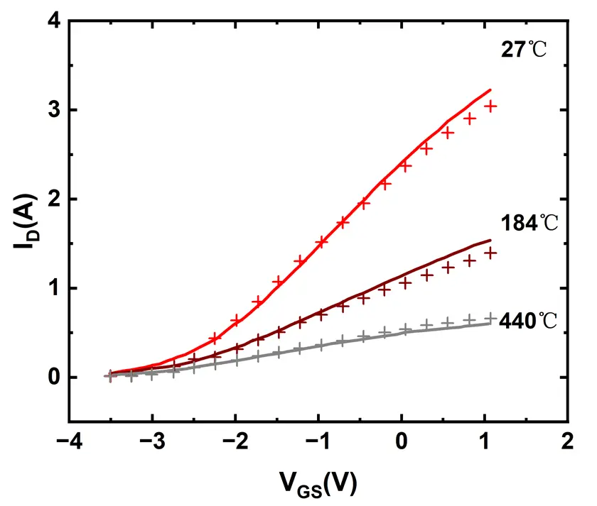
The IV models of GaN HEMTs include empirical models, semi-empirical models, etc. [30,31,32,33,34]. Figure 7 shows high-temperature ID-VGS prediction curves of HEMTs based on a semi-empirical model [35] and the experimental verification results, indicating good agreement. By integrating this model into the temperature simulator [36], the high-temperature failure mechanism of GaN HEMTs was found to be related to the drain-gate leakage current associated with the Schottky gate.
Time Dependent Dielectric Breakdown (TDDB) is one of the important tests to evaluate the reliability of power devices. Warnock [37] investigated the temperature dependence of TDDB in GaN MIS-HEMTs and found that both t1BD(time-to-first breakdown) and tHBD(time-to-hard breakdown) significantly decrease as the temperature increases to 150 ℃. In another study [38], when the MIS-HEMT was in the Progressive Breakdown(PBD) stage, IG exhibited a power-law dependence and a temperature dependence under negative gate bias, along with dual-exponential behavior at high temperatures, such as 125 ℃.
2.3. The HT Characteristics of P-GaN HEMTs
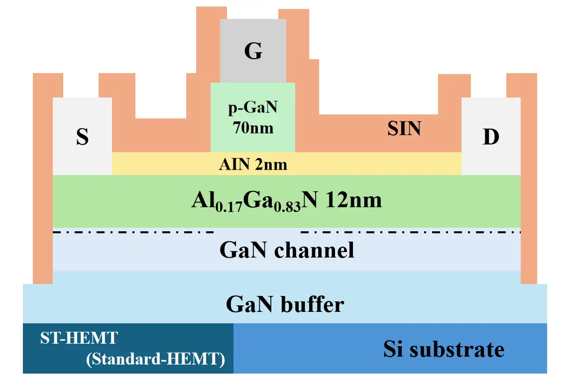
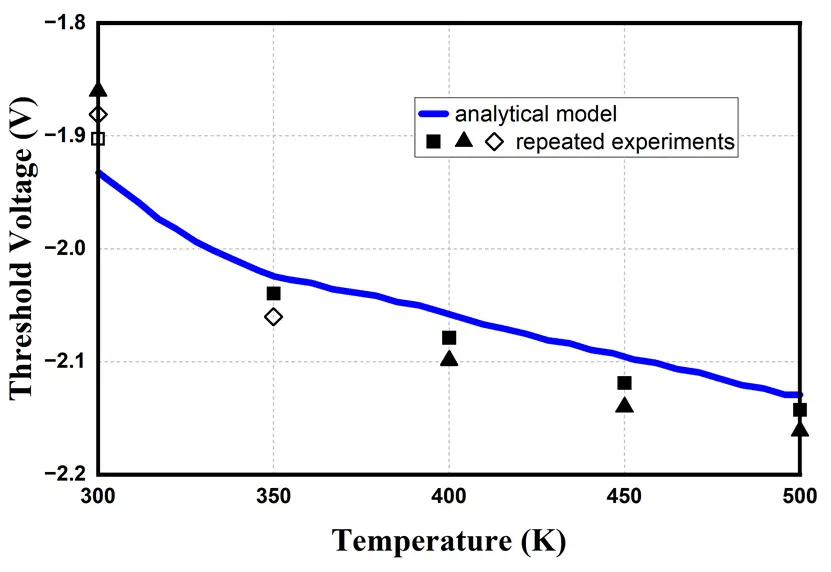
Liu et al. [39] proposed a p-GaN gated AlGaN/GaN HEMTs with HR-GaN layers that can suppress a positive shift at 500 K, as illustrated in Figure 8. Clément et al. [40] studied the impact of temperature on the performance of p-GaN HEMTs on Si and SiC substrates. When the temperature increases from 20 ℃ to 420 ℃, the saturation current decreases by 70%, and Ron increases by approximately five times. The results indicate that the different substrates and doping hardly effect the threshold voltage change. Above 200 ℃, the temperature-dependent threshold is around Δ = 0.125 mV/℃. In p-GaN gate HEMTs, Vth shift is mainly caused by the interface state of p-GaN layer and the GaN buffer at high temperatures. Ron increases and gm decreases due to the degradation of electron mobility at high temperatures.
Reference [41] reported the degradation behaviour and physical mechanism of the AlGaN/GaN HEMTs with a p-GaN gate after High-Temperature Gate Bias (HTGB) stress at 150 ℃. The results indicate that the threshold voltage and gate leakage current experienced a significant increase, while the saturation current obviously decreased after the HTGB stress. However, the on-state resistance and reverse characteristics remained unchanged. Similar gate degradation mechanisms were reported in reference [42], which proposed that both the gate breakdown voltage (BV) and mean-time-to-failure (MTTF) exhibit a positive temperature dependence.
Zhang et al. [43] proposed a novel Surface Reinforcement Layer (SRL) technology. Time-Dependent Gate Breakdown (TDGB) tests performed on p-GaN HEMTs at 150 °C demonstrated a higher maximum applicable gate voltage VG-max and could sustain a higher gate current IG, thereby significantly enhancing high-temperature gate reliability. This advancement paves the way for the development of more reliable p-GaN gate power devices. Meanwhile, Millesimo et al. [44] analyzed the TDGB test in p-GaN HEMTs at high temperatures. Their work focused on investigating the impact of different isolation processes on long-term gate reliability. It revealed two distinct failure mechanisms (area-related and isolation-related) with a complex interplay between temperature and gate bias.
2.4. Other Structures of GaN Devices
In addition to conventional GaN MIS-HEMTs, some novel GaN devices are designed to facilitate the advancement of power electronics circuits under extreme thermal conditions. By positioning a floating ohmic electrode between the source and gate of the device for current sensing, as shown in Figure 9. It demonstrates a favourable current sensing ratio at temperatures ranging from 25 ℃ to 160 ℃ [45].
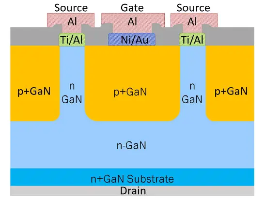
Compared to the lateral GaN HEMT, the vertical GaN Fin-JFET in Figure 10 presents some advantages, such as a higher breakdown voltage (BV) of 1.2 kV, greater current conduction capability, excellent heat dissipation capability, and lower on-resistance drift rate [46]. However, a drawback of this device is that it is challenging to be monolithically integrated, which would limit the application range.
Another GaN PIN diode structure is shown in Figure 11 [47]. The Ron of this kind of diode structure is found to become unstable under the thermal stress of 400 ℃ for a long time, which provides a reference for the reliability study of GaN vertical devices.
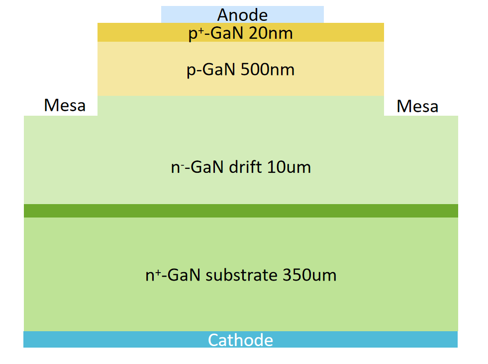
Figure 12 is the schematic cross-section of a GaN MOS-HEMT. It involves a high-quality oxide insulating layer (such as Al2O3 or SiO2) under the gate, thereby forming a gate structure similar to that of a MOSFET. This allows the GaN HEMT to maintain its high performance while benefiting from the driving simplicity and the enhanced safety features of a MOSFET.
3. The Thermal Degradation on GaN HEMTs
3.1. The Threshold Voltage Shift at High Temperatures
The threshold voltage is essential to the performance of the GaN integrated circuits, as its value can influence the on/off state of the device, potentially leading to false triggering. The GaN HEMTs with fluorine implantation are unsuitable for high-temperature applications due to the instability of fluorine concentration over prolonged exposure to high temperatures [48]. The results shown in Figure 13 manifest that the Vth of normally-on GaN HEMTs slightly decreases with elevated temperatures, which is around −1 mV/℃ [49].
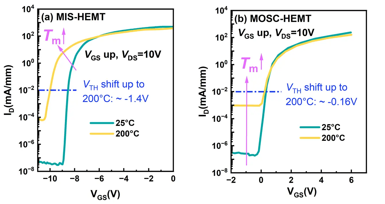
However, the introduction of a gate insulator leads to a significant change in the Vth shift, which is ascribed to the surface traps in the AlGaN [50]. The mechanisms of threshold voltage shift are different under various temperature conditions. From room temperature to 100 ℃, the dominant factor is the traps in the AlGaN barrier, while the threshold voltage shift is more susceptible to the insulator/semiconductor interface traps above 100 ℃ [51]. To reveal the mechanism of thermally-induced threshold voltage shift in MIS-HEMTs and MOSC-HEMTs, He et al. [52] compared the performance of MIS-HEMTs and MOSC-HEMTs with the same dielectric layer, and the results indicate that the Vth shift of MOSC-HEMTs under 200 ℃ is significantly smaller, as depicted in Figure 14.
Moreover, the threshold voltage shift can vary depending on the type of insulator used. For instance, a positive shift can be found with high-κ materials, like Gd2O2 [53] or ZrO2 [54], while a negative shift was observed with the moderate-κ material (Al2O3) [52]. Moreover, the same material grown by different deposition processes can result in different Vth shifts, such as Al2O3 grown by the reactive-ion-sputtered method and atomic layer deposition [55]. The p-GaN gate device also presents a bidirectional voltage shift with different gate types [56]. At elevated temperatures, a positive Vth shift was observed in a Schottky-type device, while a negative Vth shift was observed in an Ohmic-type device [57].
3.2. The Saturation Current at High Temperatures
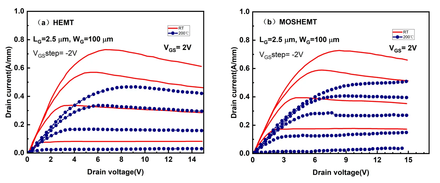
The saturation current of GaN-based devices on different substrates, such as SiC and sapphire, significantly decreases with increasing temperature [58,59]. The reduction of output saturation current at high temperatures is caused by phonon scattering [60], resulting in a low carrier mobility [61]. In reference [62], an analytical expression was proposed to calculate the saturation current under different temperature conditions. Husna et al. reported that the introduction of an insulator has a minimal effect on the saturation current in reference [63]. As shown in Figure 15, the saturation current of GaN HEMT and GaN MOS-HEMT decreased by 33% and 32%, respectively, when the test temperature was raised to 200 ℃.
Moreover, the magnitude of the drain-source current is determined by two factors, carrier sheet density and effective carrier mobility [64]. However, the carrier sheet density remains unchanged at different temperatures in reference [65,66]. Hence, carrier mobility, which is influenced by phonon scattering, is the key factor determining the saturation current. On the other hand, the DC characteristics illustrate that the recessed E-mode GaN HEMT yields a decreased saturation current with elevated temperatures [67]. The transfer curve of p-GaN HEMTs under high temperatures was measured by Keysight 1500 [68]. As illustrated in Figure 16, it can be inferred that the saturation current of p-GaN gate devices decreases due to the elevated test temperature. Concurrently, the on-state resistance experiences an increase, while the trans-conductance undergoes a decrease at elevated temperatures. This phenomenon can be attributed to the reduction in electron mobility. In summary, the saturation current of GaN devices decreases at elevated temperatures, and the gate transconductance is significantly influenced by the electron velocity, which decreases at high temperatures [69]. The transconductance of GaN HEMTs decreases at increased temperatures [70], indicating that the gate control ability degrades under high temperatures.
3.3. The Leakage Currents at High Temperatures
The leakage current was observed to exhibit both negative and positive trends in GaN HEMTs at elevated temperatures. Arulkumaran et al. investigated the mechanism of forward leakage current and found that leakage current decreases with temperatures up to 80 ℃ [71] in Figure 17, and the negative coefficient of leakage current from 20 ℃ to 70 ℃ is due to the impact ionisation [72]. The electrical field of impact ionisation has a positive temperature coefficient, which leads to a reduction in the hole leakage current with increased temperatures [73]. The positive temperature dependence of the gate leakage current is due to the surface hopping conduction mechanism [73] and temperature-assisted tunnelling mechanism [74]. The post-gate annealing was proposed in reference [75] to reduce the gate leakage current by removing shallow traps and activating deeper traps. The reverse-bias leakage current was analysed in reference [76], and the results indicated that the leakage current is dominated by trap-assisted tunnelling transport below 500 K, while thermionic field emission becomes dominant from 500 K to 600 K. The leakage current under high temperatures can be reduced by the introduction of a gate dielectric layer. Figure 18 shows the leakage current of GaN HEMTs and MIS HEMTs at various temperatures [22]. The leakage current of MIS HEMTs is two orders of magnitude smaller than that of HEMTs at 600 ℃. Liu et al. [77] studied the mechanism of forward gate leakage current in Al2O3/AlGaN/GaN metal-oxide-semiconductor HEMTs (MOS-HEMTs), and the results illustrate that Fowler-Nordheim (F-N) tunnelling is dominant at low temperatures(T < 0 ℃), while trap-assisted tunnelling (TAT) prevails from 0 ℃ to 200 ℃. Xu et al. found that the dominant leakage mechanism in p-GaN devices is the thermionic field emission caused by high-leakage Schottky contacts, whereas Poole-Frenkel emission(PFE) dominates in low-leakage Schottky contacts [78].
3.4. The Dynamic Resistance at High Temperatures
The degradation of dynamic ON-resistance (dynamic RON) is a major challenge for GaN HEMTs in power applications, originating from buffer traps, surface states, and threshold voltage (VTH) shift. Tanaka [79] indicated that high temperatures from 100 ℃ to 200 ℃ can lead to an increase in the dynamic ON-resistance of GaN HEMTs. Li [80] proposed a novel p-GaN drain (PD) structure, which improved the high-temperature degradation of dynamic RON. With this structure, the GaN enhancement-mode HEMT (E-HEMT) can achieve enhanced hole compensation at elevated temperatures, resulting in superior dynamic ON-resistance performance. Rathaur [81] demonstrated a quaternary InAlGaN/GaN MIS-HEMT with excellent initial performance and high-temperature stability, exhibiting only a 29% degradation in dynamic ON-resistance at 150 ℃.
3.5. The Metallization at High Temperatures
Incorporating titanium nitride (TiN) into the ohmic metal layer of a HEMT has been demonstrated to enhance the thermal stability of the ohmic contact. Zhu et al. [82] proposed ohmic contacts with TiN/Ti/Pt/Au and TiN/Pt/Au. The performance of the TiN/Pt/Au ohmic contact demonstrates minimal sensitivity to variations in annealing temperature. In contrast, the specific contact resistance of the TiN/Ti/Pt/Au ohmic contact exhibits a modest increase with increasing annealing temperature. The good temperature stability of regrown contacts and alloyed contacts was evaluated using TEM and TLM testing by Niroula et al [83]. The results indicated that prolonged exposure to high-temperature environments did not cause significant degradation of crystal structure or metallization properties. This study proposes an ohmic contact technology solution for gallium nitride transistors operating in high-temperature environments. Zhang et al. [84] proposed a Au-free Ti/Al/Ti/TiN ohmic contact annealed at 550 ℃, which achieved a smaller contact resistance and specific contact resistivity, while avoiding the AlGaN surface nitrogen vacancy defects and oxidation issues caused by traditional high-temperature annealing. High-temperature environments present a significant challenge for HEMTs, as they are susceptible to degradation of the gate metals. Rasel et al. [85] observed a significant reduction in gate contact area at 470 ℃, along with Ni/Au intermixing near the gate/AlGaN interface. Klein et al. [86] examined the high-temperature thermal stability of three gate metal stacks. The following gate types are distinguished: W-gate, Pd-gate, and Pt/Au-gate. At 600 ℃, the Pt/Au-gate stack demonstrated the minimal Vth drift and the most substantial Ion/Ioff discrepancy, thereby substantiating its preeminence as the optimal selection for gate metal.
4. Application of GaN Circuits at High Temperatures
Figure 19 shows a summary of high-temperature GaN integrated circuits, and there is an upward trend in the maximum operating temperature of GaN circuits. The maximum operating temperature of complex circuits remains between 200 ℃ and 350 ℃. The GaN circuits can be integrated on different substrate materials, such as Si, SiC, and diamond. The GaN on Si substrate was used in references [87,88], and the operating temperature of GaN circuits can surpass 500 ℃. These results indicate an increasing trend of GaN integrated circuits for high-temperature operations.
4.1. Power Supply Circuits
Owing to the high electron mobility and good thermal conductivity of GaN material, power supply circuits based on GaN devices are proper for high temperature and high-frequency applications. A GaN voltage reference generator based on fluorine ion implantation achieves a negative reference voltage (−2 V), and the average drift of the reference voltage is less than 0.5 mV/℃ from 25 ℃ to 250 ℃ [89]. However, the positive reference voltage is more desirable for power electronics to ensure safety operation. Hence, a reference generator based on MIS-HEMT technology was proposed with a positive supply voltage (2.53 V), and the temperature coefficient of this work is 26.2 ppm/℃ [90]. The proportional to absolute temperature (PTAT) voltage source incorporates F-ion-based GaN devices, demonstrating a maximum operating temperature of 250 ℃, and the average temperature drift of this voltage source is 0.35 mV/°C [91]. Moreover, Liao et al. proposed a reference generator based on p-type gate GaN HEMTs with a temperature coefficient of 23.6 ppm/℃ from -50 to 200 ℃ [92]. Cao et al. proposed a reference generator with a temperature coefficient of 22.1 ppm/℃ [93].
4.2. Comparators
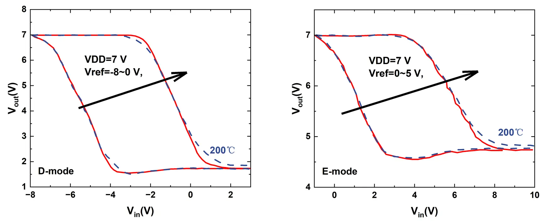
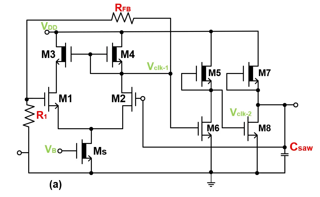
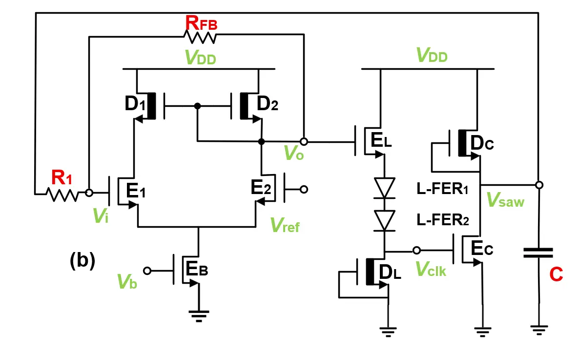
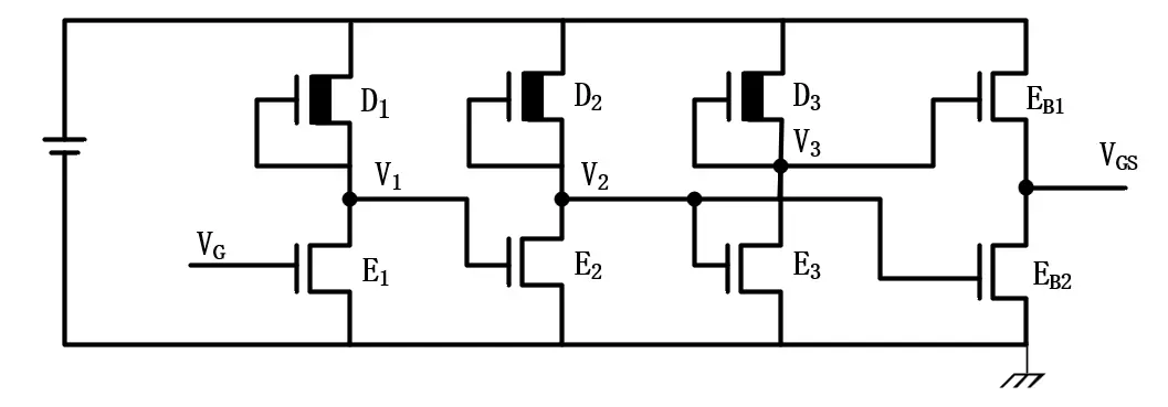
In integrated circuits, comparators play a crucial role in performing essential functions such as signal comparison and level conversion. Table 1 lists the voltage gain, bandwidth, and voltage comparison range of various GaN comparators at high temperatures. Most of the comparators are amplifiers with differential pairs. When one input of the differential pair is connected to a reference voltage, the other is the sampling signal, thus realizing the functionality of the comparator. The comparator in reference [94] is based on fluorine ion implantation technology, and it demonstrates a gain exceeding 31 dB and a bandwidth surpassing 4 MHz at 250 ℃. The performance of the comparator that utilizes the same gate process technology is superior, achieving a higher voltage gain of 32 dB and a bandwidth of 2.47 MHz at 250 ℃ [95]. Additionally, the voltage comparison range has been expanded to 1–6 V [95]. This comparator was utilized to achieve a sawtooth generator and a pulse width modulation (PWM) [96]. The MIS-HEMT technology can reduce the leakage current and improve the performance of GaN devices. A monolithically integrated GaN comparator based on MIS-HEMTs achieves an extended voltage comparison range (3 to 9 V) from RT to 250 ℃ [97]. In reference [98], the differential pairs include two E-mode GaN MIS-HEMTs, and the performance of the comparator with D-mode differential pairs was also evaluated. The comparison range is from −8 V to 0 V and 0 V to 5 V for D-mode and E-mode differential pairs, respectively. Both comparators can operate at 200 ℃, as indicated in Figure 20. Moreover, a 2-step comparator based on p-GaN gate devices was proposed in reference [99] with a gain of 53 dB at 200 ℃. As the temperature increases, the GaN comparators exhibit a decreasing trend in the voltage gain, which is attributed to the reduction in effective conductance of GaN devices. Based on GaN comparators, several complex integrated circuits were proposed. A GaN sawtooth generator in Figure 21a can produce a high-amplitude sawtooth signal at 500 kHz with a magnitude of 6.1 V at 250 ℃ [97]. Moreover, the GaN sawtooth generator in Figure 21b can be applied to generate a PWM circuit. This work is capable of generating a 1 MHz signal at 250 ℃, and the duty cycle of the signal is efficiently modulated by the reference voltages with excellent linearity [96].
Table 1. A list of GaN comparators at high temperatures.
Reference |
Year |
Technology |
Temperature |
Voltage Gain |
Bandwidth |
Comparison Range |
|---|---|---|---|---|---|---|
[94] |
2011 |
F-implantation |
250 ℃ |
>31 dB |
>4 MHz |
0.5–2 V |
[95] |
2011 |
F-implantation |
250 ℃ |
32.0 dB |
2.47 MHz |
1–6 V |
[96] |
2015 |
F-implantation |
250 ℃ |
- |
- |
0.6–2 V |
[97] |
2021 |
MIS-HEMT |
250 ℃ |
- |
- |
3–9 V |
[98] |
2021 |
MIS-HEMT |
200 ℃ |
- |
- |
0–5 V |
[99] |
2025 |
p-type gate |
200 ℃ |
53 dB |
- |
4–7 V |
4.3. Inverters
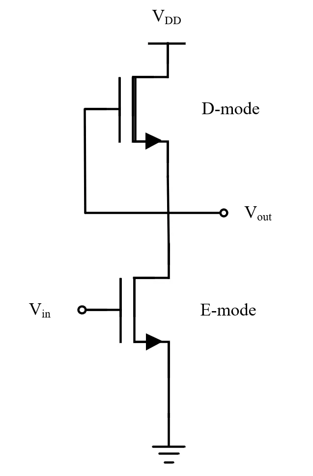
A GaN inverter was proposed in reference [12], serving as a fundamental logic block in digital circuits. It consists of a D-mode GaN HEMT and an E-mode GaN HEMT to construct a direct coupled FET logic (DCFL), as illustrated in Figure 22. Table 2 compares the operating temperatures and logic high/low noise margins of different GaN inverters.
Table 2. A list of GaN inverters at high temperatures.
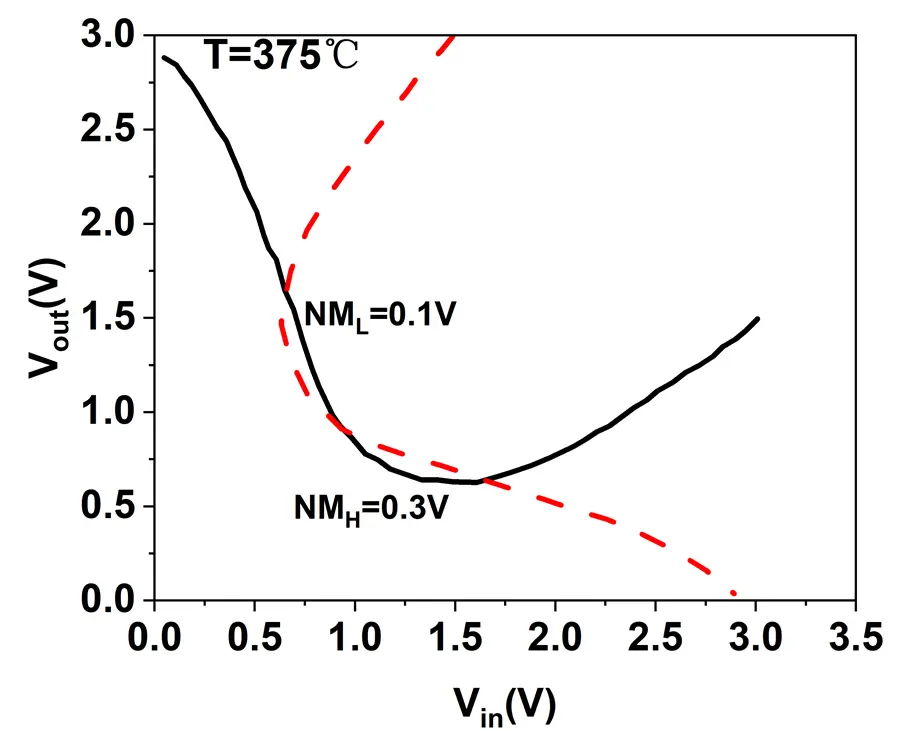
Although the temperature increases to 375 ℃, the GaN inverter in reference [12] consistently operates with a logic low noise margin (NML) of 0.1 V and a logic high noise margin (NMH) of 0.3 V, as shown in Figure 23. The fluorine ion implantation GaN inverter degrades at high temperatures due to the poor thermal stability of F- ion in the AlGaN layer.
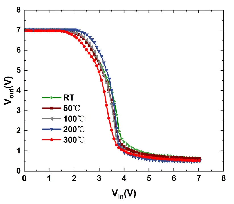
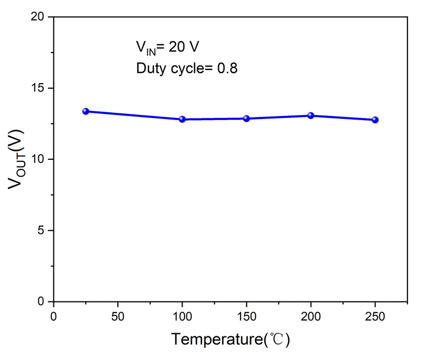
To improve the high temperature performance, the inverter incorporates a gate-recessed E-mode GaN HEMT, which improves NML and NMH to 2.4 V and 3.4 V with a voltage swing of 6.5 V, respectively [100]. Figure 24 shows that a VOH of 7 V and a VOL of 0.5 V are achieved at 300 ℃, indicating good performance at high temperatures.
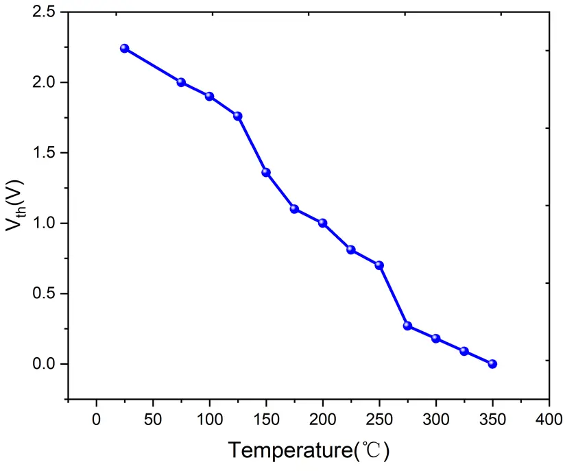
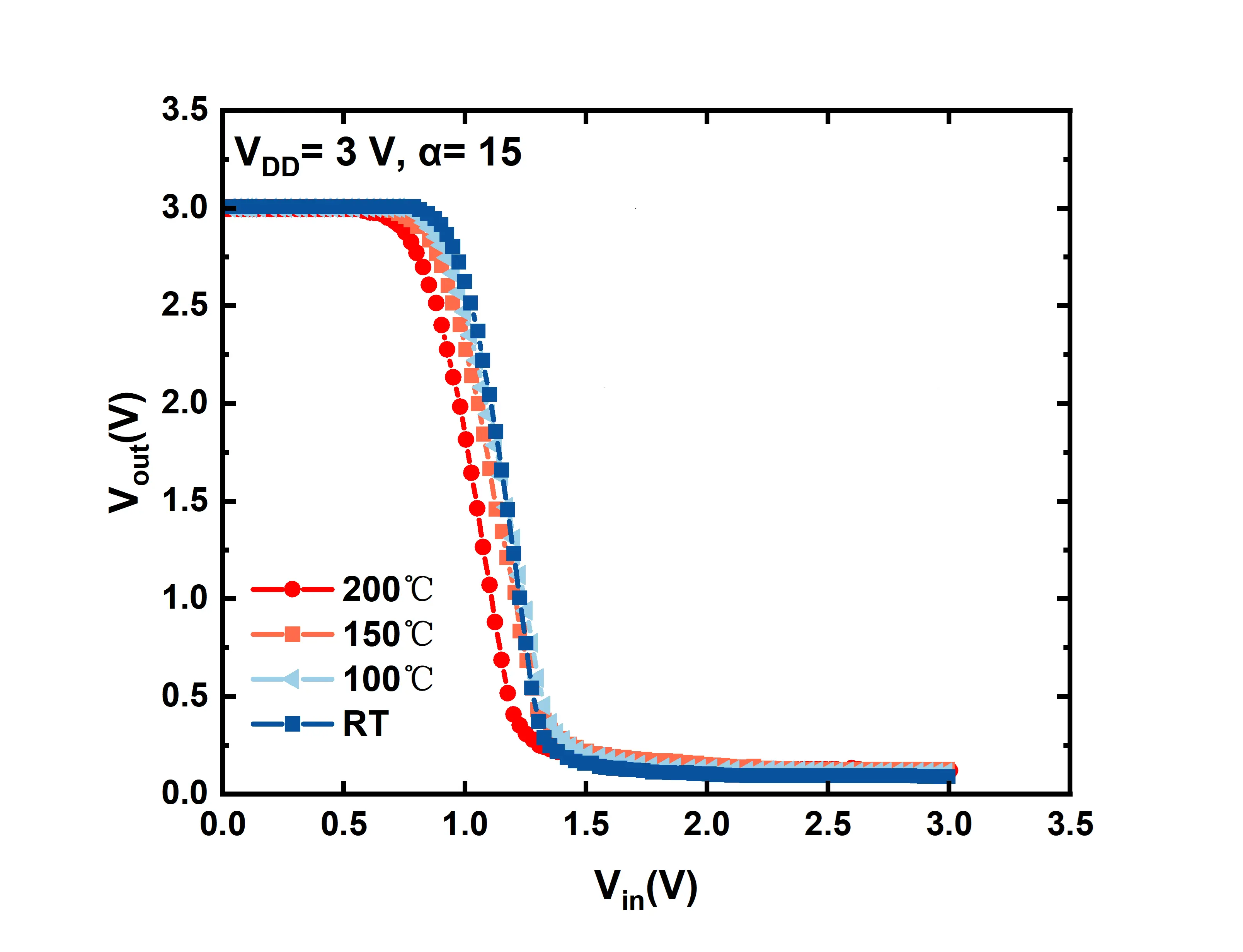
The DCFL inverter based on MIS-HEMTs can reduce the off-state leakage current at high temperatures, which increases its operation temperature to 400 ℃ [87]. In reference [101], the p-type GaN device was fabricated on the diamond substrate. The inverter consists of an n-type D-mode MIS-HEMT and a p-type diamond GaN device, and it exhibits robust functionality even under a high temperature of 350 ℃. As depicted in Figure 25, from 25 °C to 350 °C, the MIS-HEMT inverter experienced a Vth drift of approximately 2.4V. The p-GaN gate technology was also applied in the inverter circuit, with a maximum operation temperature of 200 ℃ [102]. The high temperature performance of the p-type GaN inverter degrades as the threshold voltage of the p-type device decreases in Figure 26. The maximum temperature of the GaN inverter, as reported in reference [103], is based on GaN 500 technology, which has a maximum operation temperature of 500 ℃.
The load-Shift Ketyig (LSK) demodulator, based on the inverter proposed in reference [103], remains fully operational at elevated temperatures up to 400 ℃. It can detect a minimum amplitude difference of 1 V between the high voltage level (HVL = ±5 V) and the low voltage level (LVL = ±4 V) of the modulated signal, with a total power of 3.4 W. Based on the DCFL inverter [12], a 17 stage ring oscillator was proposed. The operation temperature of the oscillator is 375 ℃.
4.4. Temperature Sensors
Compared to traditional Si MOSFETs, GaN devices are preferred for high-temperature sensors owing to their high temperature tolerance, excellent electron mobility, and compatibility with high-power applications. The temperature sensors based on F-ion implantation technology were proposed in [104] with a temperature sensitivity of −6.9 mV/℃. However, the temperature sensor based on the same gate process can achieve a temperature sensitivity of 0.35 mV/℃ with a smaller area (0.207 mm2) [91]. Both sensors operate within a temperature range of 25 ℃ to 250 ℃. These two temperature sensors present the change of temperature at different voltage levels. Another method to reflect temperature variation involves using resistors with a sensitivity of 10 Ω/℃ from 25 ℃ to 175 ℃ [105]. Moreover, the temperature sensor based on a GaN Schottky barrier diode can work from 25 ℃ to 200 ℃ [106]. The GaN MIS-HEMT temperature sensor with a sensitivity of 15.86 mV/℃ was proposed in reference [107] with a circuit area of 0.05 mm2. The temperature sensor based on a p-GaN/AlGaN/GaN heterostructure with a sensitivity of 19.7 mV/℃ was proposed in reference [108]. The detailed comparison of GaN temperature sensors is listed in Table 3.
Table 3. Performance summary of GaN temperature sensors.
Reference |
Year |
Technology |
Temperature Range (℃) |
Temperature Sensitivity (mV/℃) |
Area (mm2) |
|---|---|---|---|---|---|
[104] |
2013 |
F-implantation |
25–275 ℃ |
−6.9 |
1.23 |
[91] |
2014 |
F-implantation |
25–250 ℃ |
0.35 |
0.207 |
[105] |
2016 |
GaN HEMT |
25–175 ℃ |
10 |
- |
[106] |
2020 |
GaN SBD |
25–200 ℃ |
1.6 |
0.2 |
[107] |
2023 |
MIS-HEMT |
25–250 ℃ |
15.86 |
0.05 |
[108] |
2023 |
P-GaN/AlGaN/GaN |
25–300 ℃ |
19.7 |
- |
4.5. GaN DC-DC Converters
To fully realise the advantages of GaN devices at high temperatures, monolithic GaN DC-DC converters for high-temperature applications were proposed [109,110]. In Reference [109], a gate driver for GaN DC-DC converters was designed as shown in Figure 27. The GaN gate driver circuit includes DFCL inverters and a buffer stage, and the converter shows only 11% reduction of the output voltage at 250 ℃. Based on this driver design, Cui et al. proposed a synchronous buck converter with good thermal stability from 25 ℃ to 250 ℃, as shown in Figure 28 [110]. At high temperatures, the turn-on and turn-off processes of the GaN device become slow due to the reduction of charging and discharging currents. Consequently, the high-side and low-side power transistors may be simultaneously conducted. To ensure safe operation of DC-DC converters at high temperatures, a monolithically integrated GaN deadtime generator was proposed for GaN DC-DC buck converters in reference [111]. The results indicate that a deadtime of less than 0.13 µs is achieved at 250 ℃, and the peak efficiency of the proposed converter is 80% at high temperatures. In Reference [112], an active clamp flyback inverter achieved a switching frequency of 800 kHz at 200 °C. Martijn et al. verified the hypothesis that switching capacitance increases at high temperatures and affects power losses in a half-bridge switching stage [113]. These results validate the advantages of GaN devices and integrated circuits for high-temperature power converters in applications under extreme environments.
5. Conclusions
GaN demonstrates significant potential as a material for power electronics, particularly in high-temperature semiconductor applications. This review summarises GaN device properties and applications at various temperatures, including saturation current, leakage current, on-state resistance, transconductance, and threshold voltage. Solutions are summarised to reduce the temperature drift of specific parameters. The review also offers a comprehensive discussion on thermal degradation mechanisms of their properties. Furthermore, the performance of GaN integrated circuits at various temperatures is reviewed to investigate their potential for temperature applications. Despite the acceptable performance degradation at high temperatures, the thermal reliability of GaN devices, along with their ability to operate at higher frequencies, positions them as a promising candidate for high frequency and high efficiency power electronics under extreme environments.
Author Contributions
K.Z.: Validation, Visualization, Writing—Original Draft, and Writing—Review & Editing; P.C.: Validation, Visualization, Writing—Original Draft, and Writing—Review & Editing; J.J.: Validation, and Writing—Review & Editing; Y.X.: Review & Editing; Z.L.: Review & Editing; F.X: Review & Editing; M.C.: Supervision, Project Administration, and Writing—Review & Editing.
Ethics Statement
Not applicable.
Informed Consent Statement
Not applicable.
Data Availability Statement
All data included in this study are available upon request by contact with the corresponding author.
Funding
This work was supported by XJTLU Research Development Fund (RDF21-02-031, PGRS2206039).
Declaration of Competing Interest
The authors declare that they have no known competing financial interests or personal relationships that could have appeared to influence the work reported in this paper.
References
-
Qi F, Xu L. Development of a High-Temperature Gate Drive and Protection Circuit Using Discrete Components. IEEE Trans. Power Electron. 2017, 32, 2957–2963. doi:10.1109/TPEL.2016.2573643. [Google Scholar]
-
Hassan A, Savaria Y, Sawan M. Electronics and Packaging Intended for Emerging Harsh Environment Applications: A Review. IEEE Trans. Very Large Scale Integr. (VLSI) Syst. 2018, 26, 2085–2098. doi:10.1109/TVLSI.2018.2834499. [Google Scholar]
-
Shur M. Wide band gap semiconductor technology: State-of-the-art. Solid-State Electron. 2019, 155, 65–75. doi:10.1016/j.sse.2019.03.020. [Google Scholar]
-
Zhang M, Guo Z, Huang Y, Li Y, Ma J, Xia X, et al. Study of AlGaN/GaN Vertical Superjunction HEMT for Improvement of Breakdown Voltage and Specific On-Resistance. IEEE Access 2021, 9, 9895–9902. doi:10.1109/ACCESS.2021.3049374. [Google Scholar]
-
Chow TP. Wide bandgap semiconductor power devices for energy efficient systems. In Proceedings of the 2015 IEEE 3rd Workshop on Wide Bandgap Power Devices and Applications (WiPDA), Blacksburg, VA, USA, 2–4 November 2015, pp. 402–405. doi:10.1109/WiPDA.2015.7369328. [Google Scholar]
-
Millán J, Godignon P, Perpiñà X, Pérez-Tomás A, Rebollo J. A Survey of Wide Bandgap Power Semiconductor Devices. IEEE Trans. Power Electron. 2014, 29, 2155–2163. doi:10.1109/TPEL.2013.2268900. [Google Scholar]
-
Bindra A. Wide-Bandgap-Based Power Devices: Reshaping the power electronics landscape. IEEE Power Electron. Mag. 2015, 2, 42–47. doi:10.1109/MPEL.2014.2382195. [Google Scholar]
-
Chow TP. Progress in SiC high-voltage power switching devices. In Proceedings of the 1st International Workshop on Ultra-Low-Loss Power Device Technology (UPD2000), Nara, Japan, 31 May–2 June 2000. [Google Scholar]
-
Kachi T, Kanechika M, Uesugi T. Automotive Applications of GaN Power Devices. In Proceedings of the In2011 IEEE Compound Semiconductor Integrated Circuit Symposium (CSICS) 2011, Waikoloa, HI, USA, 16–19 October 2011; pp. 1–3. doi:10.1109/CSICS.2011.6062459. [Google Scholar]
-
Mitova R, Ghosh R, Mhaskar U, Klikic D, Wang M-X, Dentella A. Investigations of 600-V GaN HEMT and GaN Diode for Power Converter Applications. IEEE Trans. Power Electron. 2014, 29, 2441–2452. doi:10.1109/TPEL.2013.2286639. [Google Scholar]
-
Hassan A, Savaria Y, Sawan M. GaN Integration Technology, an Ideal Candidate for High-Temperature Applications: A Review. IEEE Access 2018, 6, 78790–78802. doi:10.1109/ACCESS.2018.2885285. [Google Scholar]
-
Cai Y, Cheng Z, Yang Z, Tang CW, Lau KM, Chen KJ. High-Temperature Operation of AlGaN/GaN HEMTs Direct-Coupled FET Logic (DCFL) Integrated Circuits. IEEE Electron Device Lett. 2007, 28, 328–331. doi:10.1109/LED.2007.895391. [Google Scholar]
-
Cai Y, Cheng ZQ, Tang WCW, Chen KJ, Lau KM. Monolithic integration of enhancement-and depletion-mode AlGaN/GaN HEMTs for GaN digital integrated circuits. In Proceedings of the IEEE International Electron Devices Meeting, Washington, DC, USA, 5–7 December 2005; Volume 774. doi:10.1109/IEDM.2005.1609468. [Google Scholar]
-
Cai Y, Zhou Y, Chen KJ, Lau KM. High-performance enhancement-mode AlGaN/GaN HEMTs using fluoride-based plasma treatment. IEEE Electron Device Lett. 2005, 26, 435–437. doi:10.1109/LED.2005.851122. [Google Scholar]
-
Wang R, Cai Y, Chen KJ. Temperature dependence and thermal stability of planar integrated enhancement/depletion mode AlGaN/GaN HEMTs and digital circuits. Solid-State Electron. 2009, 53, 1–6. [Google Scholar]
-
Badawi N, Hilt O, Bahat-Treidel E, Böcker J, Würfl J, Dieckerhoff S. Investigation of the Dynamic On-State Resistance of 600 V Normally-Off and Normally-On GaN HEMTs. IEEE Trans. Ind. Appl. 2016, 52, 4955–4964. doi:10.1109/TIA.2016.2585564. [Google Scholar]
-
Gaska R, Chen Q, Yang J, Osinsky A, Khan MA, Shur MS. High-temperature performance of AlGaN/GaN HFETs on SiC substrates. IEEE Electron Device Lett. 1997, 18, 492–494. [Google Scholar]
-
Maeda N, Saitoh T, Tsubaki K, Nishida T, Kobayashi N. Superior pinch-off characteristics at 400 °C in AlGaN/GaN heterostructure field effect transistors. Jpn. J. Appl. Phys. 1999, 38, L987–L989. [Google Scholar]
-
Arulkumaran S, Egawa T, Ishikawa H, Jimbo T. High-temperature effects of AlGaN/GaN high-electron-mobility transistors on sapphire and semi-insulating SiC substrates. Appl. Phys. Lett. 2002, 80, 2186–2188. [Google Scholar]
-
Cuerdo R, Calle F, Braña AF, Cordier Y, Azize M, Baron N, et al. High temperature behaviour of GaN HEMT devices on Si(111) and sapphire substrates. Phys. Status Solidi C 2008, 5, 1971–1973. [Google Scholar]
-
Islam AE, Sepelak NP, Miesle AT, Lee H, Snure M, Nikodemski S, et al. Effect of high temperature on the performance of AlGaN/GaN T-gate high-electron mobility transistors with 140-nm gate length. IEEE Trans. Electron Devices 2024, 71, 1805–1811. [Google Scholar]
-
Suria ASYJA, So H, Senesky DG. DC characteristics of ALD-grown Al2O3/AlGaN/GaN MIS-HEMTs and HEMTs at 600 °C in air. Semicond. Sci. Technol. 2017, 31, 115017. [Google Scholar]
-
Wang Y-H, Liang Y-C, Samudra G-S, Huang H, Huang B-J, Huang S-H, et al. 6.5 V High Threshold Voltage AlGaN/GaN Power Metal-Insulator-Semiconductor High Electron Mobility Transistor Using Multilayer Fluorinated Gate Stack. IEEE Electron Device Lett. 2015, 36, 381–383. doi:10.1109/LED.2015.2401736. [Google Scholar]
-
Wang YH, Liang YC, Samudra GS, Chu PJ, Liao YC, Huang CF, et al. High-temperature studies of multiple fluorinated traps within an Al2O3 gate dielectric for E-mode AlGaN/GaN power MIS-HEMTs. Semicond. Sci. Technol. 2015, 31, 025004. doi:10.1088/0268-1242/31/2/025004. [Google Scholar]
-
He J, Hua M, Zhang Z, Chen KJ. Performance and VTH Stability in E-Mode GaN Fully Recessed MIS-FETs and Partially Recessed MIS-HEMTs With LPCVD-SiNₓ/PECVD-SiNₓ Gate Dielectric Stack. IEEE Trans. Electron Devices 2018, 65, 3185–3191. doi:10.1109/TED.2018.2850042. [Google Scholar]
-
Liu C, Yang S, Liu S, Tang Z, Wang H, Jiang Q. et al. Thermally Stable Enhancement-Mode GaN Metal-Isolator-Semiconductor High-Electron-Mobility Transistor with Partially Recessed Fluorine-Implanted Barrier. IEEE Electron Device Lett. 2015, 36, 318–320. doi:10.1109/LED.2015.2403954. [Google Scholar]
-
Khandelwal S, Fjeldly TA. A physics based compact model for drain current in AlGaN/GaN HEMT devices. In Proceedings of the 2012 24th International Symposium on Power Semiconductor Devices and ICs, Bruges, Belgium, 3–7 June 2012; pp. 241–244. doi:10.1109/ISPSD.2012.6229068. [Google Scholar]
-
Dasari P, Bhattacharya S, Karmalkar S. Augmentation and Assessment of a Universal FET I–V Model for Simulating GaN HEMTs. IEEE Trans. Electron Devices 2020, 67, 847–854. doi:10.1109/TED.2020.2966546. [Google Scholar]
-
Dasari P, Bhattacharya S, Karmalkar S. DC extraction of the temperature dependency of low field channel mobility and parasitic resistances in a GaN HEMT. In Proceedings of the 2017 International Conference on Electron Devices and Solid-State Circuits (EDSSC), Hsinchu, Taiwan, China, 18–20 October 2017; pp. 1–2. doi:10.1109/EDSSC.2017.8126533. [Google Scholar]
-
Cheng X, Wang Y. A Surface-Potential-Based Compact Model for AlGaN/GaN MODFETs. IEEE Trans. Electron Devices 2011, 58, 448–454. doi:10.1109/TED.2010.2089690. [Google Scholar]
-
Angelov I, Zirath H, Rosman N. A new empirical nonlinear model for HEMT and MESFET devices. IEEE Trans. Microwave Theory Tech. 1992, 40, 2258–2266. doi:10.1109/22.179888. [Google Scholar]
-
Lee K, Shur MS, Drummond TJ, Morkoc H. Current–Voltage and capacitance–Voltage characteristics of modulation-doped field-effect transistors. IEEE Trans. Electron Devices 1983, 30, 207–212. doi:10.1109/T-ED.1983.21101. [Google Scholar]
-
Li M, Wang Y. 2-D Analytical Model for Current–Voltage Characteristics and Transconductance of AlGaN/GaN MODFETs. IEEE Trans. Electron Devices 2008, 55, 261–267. doi:10.1109/TED.2007.911076. [Google Scholar]
-
Cheng X, Li M, Wang Y. Physics-Based Compact Model for AlGaN/GaN MODFETs with Close-Formed I–V and C–V Characteristics. IEEE Trans. Electron Devices 2009, 56, 2881–2887. doi:10.1109/TED.2009.2030722. [Google Scholar]
-
Mocanu M, Unger C, Pfost M, Waltereit P, Reiner R. Thermal Stability and Failure Mechanism of Schottky Gate AlGaN/GaN HEMTs. IEEE Trans. Electron Devices 2017, 64, 848–855. doi:10.1109/TED.2016.2633725. [Google Scholar]
-
Pfost M, Boianceanu C, Lohmeyer H, Stecher M. Electrothermal Simulation of Self-Heating in DMOS Transistors up to Thermal Runaway. IEEE Trans. Electron Devices 2013, 60, 699–707. doi:10.1109/TED.2012.2227484. [Google Scholar]
-
Warnock S, Lemus A, Joh J, Krishnan S, Pendharkar S, del Alamo JA. Time-Dependent Dielectric Breakdown in High-Voltage GaN MIS-HEMTs: The Role of Temperature. IEEE Trans. Electron Devices 2017, 64, 3132–3138. doi:10.1109/TED.2017.2717924. [Google Scholar]
-
Warnock S, del Alamo JA. Progressive breakdown in high-voltage GaN MIS-HEMTs. In Proceedings of the 2016 IEEE International Reliability Physics Symposium (IRPS), Pasadena, CA, USA, 17–21 April 2016; pp. 4A-6-1–4A-6-6. doi:10.1109/IRPS.2016.7574531. [Google Scholar]
-
Liu X, Chiu H, Liu C, Kao H, Chiu C, Wang H, et al. Normally-off p-GaN gated AlGaN/GaN HEMTs using plasma oxidation technique in access region. IEEE J. Electron Devices Soc. 2020, 8, 229–234. doi:10.1109/JEDS.2020.2975620. [Google Scholar]
-
Fleury C, Capriotti M, Rigato M, Hilt O, Wurfl J, Derluyn J, et al. High temperature performances of normally-off p-GaN gate AlGaN/GaN HEMTs on SiC and Si substrates for power applications. Microelectron. Reliab. 2015, 55, 1687–1691. doi:10.1016/j.microrel.2015.06.010 [Google Scholar]
-
Chen W, Chen YQ, Geng K. Degradation Behavior and Mechanisms of E-mode GaN HEMTs with p-GaN Gate under High Temperature Gate Bias Stress. In Proceedings of the 2021 Global Reliability and Prognostics and Health Management (PHM-Nanjing), Nanjing, China, 15–17 October 2021; pp. 1–4. doi:10.1109/PHM-Nanjing52125.2021.9612888. [Google Scholar]
-
He J, Wei J, Yang S, Wang Y, Zhong K, Chen KJ. Frequency- and Temperature-Dependent Gate Reliability of Schottky-Type p-GaN Gate HEMTs. IEEE Trans. Electron Devices 2019, 66, 3453–3458. doi:10.1109/TED.2019.2924675. [Google Scholar]
-
Zhang L, Zheng Z, Yang S, Song W, He J, Chen KJ. p-GaN Gate HEMT With Surface Reinforcement for Enhanced Gate Reliability. IEEE Electron Device Lett. 2021, 42, 22–25. [Google Scholar]
-
Millesimo M, Fiegna C, Posthuma N, Borga M, Bakeroot B, Decoutere S, et al. High-Temperature Time-Dependent Gate Breakdown of p-GaN HEMTs. IEEE Trans. Electron Devices 2021, 68, 5701–5706. [Google Scholar]
-
Sun R, Liang YC, Yeo Y-C, Zhao C. Au-Free AlGaN/GaN MIS-HEMTs With Embedded Current Sensing Structure for Power Switching Applications. IEEE Trans. Electron Devices 2017, 64, 3515–3518. doi:10.1109/TED.2017.2717934. [Google Scholar]
-
Liu J, Xiao M, Zhang R, Pidaparthi S, Cui H, Edwards A, et al. 1.2-kV Vertical GaN Fin-JFETs: High-Temperature Characteristics and Avalanche Capability. IEEE Trans. Electron Devices 2021, 68, 2025–2032. doi:10.1109/TED.2021.3059192 [Google Scholar]
-
Wang D, Mudiyanselage DH, He Z, Da B, Fu H. Instability of On-Resistance in Vertical GaN PIN Diodes Under High-Temperature and Voltage Stress. IEEE Trans. Electron Devices 2024, 71, 1681–1686. doi:10.1109/TED.2023.3344426. [Google Scholar]
-
Chen KJ, Yuan L, Wang MJ, Chen H, Huang S, Zhou Q, et al. Physics of fluorine plasma ion implantation for GaN normally-off HEMT technology. In Proceedings of the 2011 International Electron Devices Meeting, Washington, DC, USA, 5–7 December 2011; pp. 19.4.1–19.4.4. doi:10.1109/IEDM.2011.6131585. [Google Scholar]
-
Wang YH, Liang YC, Samudra GS, Chang TF, Huang CF, Yuan L, et al. Modelling temperature dependence on AlGaN/GaN power HEMT device characteristics. Semicond. Sci. Technol. 2013, 28, 125010. [Google Scholar]
-
Kordoš P, Donoval D, Florovič M, Kováč J, Gregušová D. Investigation of trap effects in AlGaN/GaN field-effect transistors by temperature dependent threshold voltage analysis. Appl. Phys. Lett. 2008, 92, 152113. [Google Scholar]
-
Kordoš P, Donoval D, Florovič M, Kováč J, Gregušová D, et al. Temperature-induced instability of the threshold voltage in GaN-based heterostructure field-effect transistors. Semicond. Sci. Technol. 2017, 32, 025017. [Google Scholar]
-
Yang S, Liu S, Liu C, Lu Y, Chen KJ. Mechanisms of thermally induced threshold voltage instability in GaN-based heterojunction transistors. Appl. Phys. Lett. 2014, 105, 223508. [Google Scholar]
-
Das A, Chang LB, Lin RM. Investigation of temperature dependent threshold voltage variation of Gd2O3/AlGaN/GaN metal-oxide-semiconductor heterostructure. AIP Adv. 2012, 2, 034501. [Google Scholar]
-
Bothe KM, von Hauff PA, Afshar A, Foroughi-Abari A, Cadien KC, Barlage DW, et al. Electrical Comparison of HfO and ZrO2 Gate Dielectrics on GaN. IEEE Trans. Electron Devices 2013, 60, 4119–4124. [Google Scholar]
-
Dutta G, Turuvekere S, Karumuri N, DasGupta N, DasGupta A, et al. Positive shift in threshold voltage for reactive-ion-sputtered Al2O3/AlInN/GaN MIS-HEMT. IEEE Electron Device Lett. 2014, 35, 1085–1087. [Google Scholar]
-
Sayadi L, Iannaccone G, Sicre S, Häberlen O, Curatola G, et al. Threshold voltage instability in p-GaN gate AlGaN/GaN HFETs. IEEE Trans. Electron Devices 2018, 65, 2454–2460. [Google Scholar]
-
Wang H, Lin Y, Jiang J, Dong D, Ji F, Zhang M, et al. Investigation of thermally induced threshold voltage shift in normally-OFF p-GaN gate HEMTs. IEEE Trans. Electron Devices 2022, 69, 2287–2292. [Google Scholar]
-
Tarakji A, Hu X, Koudymov A, Simin G, Yang J, Khan MA, et al. DC and microwave performance of a GaN/AlGaN MOSHFET under high temperature stress. Solid-State Electron. 2002, 46, 1211–1214. [Google Scholar]
-
Aubry R, Jacquet JC, Dessertenne B, Chartier E, Adam D, Cordier Y, Delage SL, et al. Thermal characterisation of AlGaN/GaN HEMTs grown on silicon and sapphire substrates based on pulsed IV measurements. Eur. Phys. J. Appl. Phys. 2003, 22, 77–82. [Google Scholar]
-
Donoval D, Florovic M, Gregusova D, Kováč J, Kordoš P. High temperature performance of AlGaN/GaN HFETs and MOSFETs. Microelectron. Reliab. 2008, 48, 1669–1672. [Google Scholar]
-
Tan WS, Uren MJ, Fry PW, Houston PA, Balmer RS, Martin T. High temperature performance of AlGaN/GaN HEMTs on Si substrates. Solid-State Electron. 2006, 50, 511–513. doi:10.1016/j.sse.2006.02.008. [Google Scholar]
-
Pérez-Tomás A, Fontserè A, Placidi M, Baron N, Chenot S, Moreno JC, Cordier Y, et al. Temperature impact and analytical modeling of the AlGaN/GaN-on-Si saturation drain current and transconductance. Semicond. Sci. Technol. 2012, 27, 125010. doi:10.1088/0268-1242/27/12/125010. [Google Scholar]
-
Husna F, Lachab M, Sultana M, Adivarahan V, Fareed Q, Khan A. High-Temperature Performance of AlGaN/GaN MOSHEMT With SiO2 Gate Insulator Fabricated on Si (111) Substrate. IEEE Trans. Electron Devices 2012, 59, 2424–2429. doi:10.1109/TED.2012.2204888. [Google Scholar]
-
Schroder DK. Semiconductor Material and Device Characterization; Wiley: Hoboken, NJ, USA, 2006. [Google Scholar]
-
Daumiller I, Kirchner C, Kamp M, Ebeling KJ, Kohn E. Evaluation of the temperature stability of AlGaN/GaN heterostructure FETs. IEEE Electron Device Lett. 1999, 20, 448–450. doi:10.1109/55.784448. [Google Scholar]
-
Medjdoub F, Carlin JF, Gonschorek M, Feltin E, Py MA, Ducatteau D, et al. Can InAlN/GaN be an alternative to high power / high temperature AlGaN/GaN devices? In Proceedings of the 2006 International Electron Devices Meeting, San Francisco, CA, USA, 11–13 December 2006; pp. 1–4. doi:10.1109/IEDM.2006.346935. [Google Scholar]
-
Rodríguez R, González B, García J, Núñez A. Electrothermal DC characterization of GaN on Si MOS-HEMTs. Solid-State Electron. 2017, 137, 44–51. doi:10.1016/j.sse.2017.08.002. [Google Scholar]
-
Li S, Liu S, Tian Y, Zhang C, Wei J, Tao X, et al. High-temperature electrical performances and physics-based analysis of p-GaN HEMT device. IET Power Electron. 2020, 13, 420–425. [Google Scholar]
-
Simin G, Tarakji A, Hu X, Koudymov A, Yang J, Khan MA, et al. High-temperature performance of AlGaN/GaN metal–oxide–semiconductor heterostructure field-effect-transistors. Phys. Status Solidi A 2001, 188, 219–222. [Google Scholar]
-
Yahyazadeh R, Hashempour Z, Marofi O. Effect of high temperature on the transconductance of AlGaN/GaN high electron mobility transistors (HEMT). Int. J. Acad. Res. 2013, 5, 78–86. doi:10.7813/2075-4124.2013/5-4/a.9. [Google Scholar]
-
Arulkumaran S, Egawa T, Ishikawa H, Jimbo T. Temperature dependence of gate–leakage current in AlGaN/GaN high-electronmobility transistors. Appl. Phys. Lett. 2003, 82, 3110–3112. [Google Scholar]
-
Oğuzman IH, Bellotti E, Brennan KF, Kolník J, Wang R, Ruden PP. Theory of hole initiated impact ionization in bulk zincblende and wurtzite GaN. J. Appl. Phys. 1997, 81, 7827–7834. [Google Scholar]
-
Tan WS, Houston PA, Parbrook PJ, Wood DA, Hill G, Whitehouse CR. Gate leakage effects and breakdown voltage in metalorganic vapor phase epitaxy AlGaN/GaN heterostructure field-effect transistors. Appl. Phys. Lett. 2002, 80, 3207–3209. [Google Scholar]
-
Kuliev A, Kumar V, Schwindt R, Selvanathan D, Dabiran AM, Chow P, et al. 0.15 μm gate-length AlGaN/GaN HEMTs with varying gate recess length. Solid-State Electron. 2003, 47, 117–122. [Google Scholar]
-
Kim H, Lee J, Liu D, Lu W. Gate current leakage and breakdown mechanism in unpassivated AlGaN/GaN high electron mobility transistors by post-gate annealing. Appl. Phys. Lett. 2005, 86, 143505. doi:10.1063/1.1899255. [Google Scholar]
-
Karmalkar S, Sathaiya DM, Shur MS. Mechanism of the reverse gate leakage in AlGaN/GaN high electron mobility transistors. Appl. Phys. Lett. 2000, 82, 3976–3978. [Google Scholar]
-
Liu ZH, Ng GI, Arulkumaran S, Maung YKT, Zhou H. Temperature-dependent forward gate current transport in atomiclayer-deposited Al2O3/AlGaN/GaN metal–insulator–semiconductor high electron mobility transistor. Appl. Phys. Lett. 2011, 98, 163501. [Google Scholar]
-
Xu N, Hao R, Chen F, Zhang X, Zhang H, Zhang P, et al. Gate leakage mechanisms in normally off pGaN/AlGaN/GaN high electron mobility transistors. Appl. Phys. Lett. 2018, 113, 152104. doi:10.1063/1.5041343. [Google Scholar]
-
Tanaka K, Ishida M, Ueda T, Tanaka T. Effects of deep trapping states at high temperatures on transient performance of AlGaN/GaN heterostructure field-effect transistors. Jpn. J. Appl. Phys. 2013, 52, 04CF07. [Google Scholar]
-
Li S, Sheng K, Yang S. Temperature-Dependent Dynamic Ron of GaN E-HEMTs: The Impact of p-GaN Drain. IEEE Trans. Electron Devices 2023, 70, 3754–3761. [Google Scholar]
-
Rathaur SK, Ma C-J, Dixit A, Lee C-T, Chang EY. Performance and Threshold Voltage Reliability of Quaternary InAlGaN/GaN MIS-HEMT on Si for Power Device Applications. IEEE Trans. Device Mater. Rel. 2024, 24, 428–436. [Google Scholar]
-
Zhu Y, Huang R, Li Z, Hao H, An Y, Liu T, et al. Interface analysis of TiN/n-GaN Ohmic contacts with high thermal stability. Appl. Surf. Sci. 2019, 481, 1148–1153. [Google Scholar]
-
Niroula J, Xie Q, Rajput NS, Darmawi-Iskandar PK, Rahman SI, Luo S, Palacios T, et al. High temperature stability of regrown and alloyed Ohmic contacts to AlGaN/GaN heterostructure up to 500 °C. Appl. Phys. Lett. 2024, 124, 202103. [Google Scholar]
-
Zhang J, Kang X, Wang X, Huang S, Chen C, Wei K, et al. Ultralow-Contact-Resistance Au-Free Ohmic Contacts with Low Annealing Temperature on AlGaN/GaN Heterostructures. IEEE Electron Device Lett. 2018, 39, 847–850. [Google Scholar]
-
Rasel MAJ, Zhang D, Chen A, Thomas M, House SD, Kuo W, et al. Temperature-induced degradation of GaN HEMT: An in situ heating study. J. Vac. Sci. Technol. B 2024, 42, 032209. [Google Scholar]
-
Klein BA, Allerman AA, Armstrong AM. Al-rich AlGaN high electron mobility transistor gate metallization study up to 600 °C in air. Appl. Phys. Lett. 2024, 124, 102103. [Google Scholar]
-
Lee H, Ryu H, Kang J, Zhu W. High Temperature Operation of E-Mode and D-Mode AlGaN/GaN MIS-HEMTs With Recessed Gates. IEEE J. Electron Devices Soc. 2023, 11, 167–173.doi:10.1109/jeds.2023.3253137. [Google Scholar]
-
Yuan M, Xie Q, Fu K, Hossain T, Niroula J, Greer JA, et al. GaN Ring Oscillators Operational at 500 °C Based on a GaN-on-Si Platform. IEEE Electron Device Lett. 2022, 43, 1842–1845.doi:10.1109/led.2022.3204566. [Google Scholar]
-
Wong K-Y, Chen W, Chen KJ. Integrated Voltage Reference Generator for GaN smart power chip technology. IEEE Trans. Electron Devices 2010, 57, 952–955.doi:10.1109/ted.2010.2041510. [Google Scholar]
-
Li A, Shen Y, Li Z, Zhao Y, Mitrovic IZ, Wen H, et al. A Monolithically Integrated 2-Transistor Voltage Reference with a Wide Temperature Range Based on AlGaN/GaN Technology. IEEE Electron Device Lett. 2022, 43, 362–365. doi:10.1109/LED.2022.3146263. [Google Scholar]
-
Kwan AM, Guan Y, Liu X, Chen KJ. A highly linear integrated temperature sensor on a GaN Smart Power IC platform. IEEE Trans. Electron Devices 2014, 61, 2970–2976.doi:10.1109/ted.2014.2327386. [Google Scholar]
-
Liao C-H, Yang SH, Liao MY, Chung KC, Kumari N, Chen KH, et al. 3.8 A 23.6ppm/°C Monolithically Integrated GaN Reference Voltage Design with Temperature Range from −50 °C to 200 °C and Supply Voltage Range from 3.9 to 24V. In Proceedings of the 2020 IEEE International Solid-State Circuits Conference—(ISSCC), San Francisco, CA, USA, 16–20 February 2020; pp. 72–74. doi:10.1109/ISSCC19947.2020.9062940. [Google Scholar]
-
Cao P, Zhao K, Xu Y, Van Zalinge H, Lam S, Zhang P, et al. A p-GaN HEMT Voltage Reference with High Line Sensitivity and Power Supply Rejection Ratio. IEEE J. Electron Devices Soc. 2025, 13, 630–637. doi:10.1109/JEDS.2025.3588210. [Google Scholar]
-
Kwan AMH, Wong KY, Liu X, Chen KJ. High-Gain and High-Bandwidth AlGaN/GaN High Electron Mobility Transistor Comparator with High-Temperature Operation. Jpn. J. Appl. Phys. 2011, 50, 04DF02. doi:10.1143/jjap.50.04df02. [Google Scholar]
-
Liu X, Chen KJ. GaN Single-Polarity Power Supply Bootstrapped Comparator for High-Temperature Electronics. IEEE Electron Device Lett. 2011, 32, 27–29. doi:10.1109/led.2010.2088376. [Google Scholar]
-
Wang H, Kwan AMH, Jiang Q, Chen KJ. A GaN Pulse Width Modulation Integrated Circuit for GaN Power Converters. IEEE Trans. Electron Devices 2015, 62, 1143–1149. doi:10.1109/TED.2015.2396649. [Google Scholar]
-
Li A, Cui M, Shen Y, Li Z, Liu W, Mitrovic IZ, et al. Monolithic Comparator and Sawtooth Generator of AlGaN/GaN MIS-HEMTs With Threshold Voltage Modulation for High-Temperature Applications. IEEE Trans. Electron Devices 2021, 68, 2673–2679. doi:10.1109/ted.2021.3075425. [Google Scholar]
-
Wang W, Li A, Cui M, Wen H, Liu W, et al. Monolithic Comparators using E/D-mode AlGaN/GaN MIS-HEMTs for High-temperature Applications. In Proceedings of the 2021 18th China International Forum on Solid State Lighting & 2021 7th International Forum on Wide Bandgap Semiconductors (SSLChina: IFWS), Shenzhen, China, 6–8 December 2021. [Google Scholar]
-
Geng Y, Zheng Z, Zhang L, Cheng Y, Chen T, Feng S, et al. Monolithically Integrated GaN Comparator Based on Complementary Logic. IEEE Trans. Electron Devices 2025, 72, 611–617. doi:10.1109/TED.2024.3517603. [Google Scholar]
-
Xu Z, Wang J, Cai Y, Liu J, Yang Z, Li X, et al. High Temperature Characteristics of GaN-Based Inverter Integrated With Enhancement-Mode (E-Mode) MOSFET and Depletion-Mode (D-Mode) HEMT. IEEE Electron Device Lett. 2014, 35, 33–35. doi:10.1109/led.2013.2291854. [Google Scholar]
-
Ren C, Malakoutian M, Li S, Chowdhury S. Hydrogen-terminated diamond FET and GaN HEMT delivering CMOS inverter operation at high-temperature. In Proceedings of the 2020 Device Research Conference (DRC), Columbus, OH, USA, 21–24 June 2020; pp. 1–2. doi:10.1109/DRC50226.2020.9135152. [Google Scholar]
-
Jia L-F, Zhang L, Xiao J-P, Cheng Z, Lin D-F, Ai Y-J, et al. E/D-Mode GaN Inverter on a 150-mm Si Wafer Based on p-GaN Gate E-Mode HEMT Technology. Micromachines 2021, 12, 617. doi:10.3390/mi12060617. [Google Scholar]
-
Hassan A, Amer M, Savaria Y, Sawan M. Fully Integrated Digital GaN-Based LSK Demodulator for High-Temperature Applications. IEEE Trans. Circuits Syst. II 2020, 67, 1579–1583. doi:10.1109/TCSII.2020.3010094. [Google Scholar]
-
Kwan AMH, Guan Y, Liu X, Chen KJ. Integrated over-temperature protection circuit for GaN smart power ICs. Jpn. J. Appl. Phys. 2013, 52, 08JN15. doi:10.7567/JJAP.52.08JN15. [Google Scholar]
-
Reiner R, Waltereit P, Weiss B, Wespel M, Meder D, Mikulla M, et al. Linear temperature sensors in high-voltage GaN-HEMT power devices. In Proceedings of the 2016 IEEE Applied Power Electronics Conference and Exposition (APEC), Long Beach, CA, USA, 20–24 March 2016; pp. 2083–2086. doi:10.1109/APEC.2016.7468154. [Google Scholar]
-
Li X, Pu T, Li X, Li L, Ao J-P. Correlation between anode area and sensitivity for the TiN/GaN Schottky barrier diode temperature sensor. IEEE Trans. Electron Devices 2020, 67, 1171–1175. doi:10.1109/TED.2020.2968358. [Google Scholar]
-
Li A, Li F, Chen K, Zhu Y, Wang W, Mitrovic IZ, et al. A Supply Voltage Insensitive Two-Transistor Temperature Sensor With PTAT/CTAT Outputs Based on Monolithic GaN Integrated Circuits. IEEE Trans. Power Electron. 2023, 38, 10584–10588. doi:10.1109/TPEL.2023.3288937. [Google Scholar]
-
Chang J, Yin Y, Du J, Wang H, Li H, Zhao C, et al. On-Chip Integrated High-Sensitivity Temperature Sensor Based on p-GaN/AlGaN/GaN Heterostructure. IEEE Electron Device Lett. 2023, 44, 594–597. [Google Scholar]
-
Cui M, Bu Q, Cai Y, Sun R, Liu W, Wen H, et al. Monolithic integration design of GaN-based power chip including gate driver for high-temperature DC–DC converters. Jpn. J. Appl. Phys. 2019, 58, 050902. doi:10.7567/1347-4065/ab1313. [Google Scholar]
-
Cui M, Sun R, Bu Q, Liu W, Wen H, Li A, et al. Monolithic GaN Half-Bridge Stages with Integrated Gate Drivers for High Temperature DC-DC Buck Converters. IEEE Access 2019, 7, 184375–184384. doi:10.1109/ACCESS.2019.2958059. [Google Scholar]
-
Cui M, Zhu Y, Cao P, Li A, Bu Q, Mitrovic IZ, et al. A monolithic GaN driver with a deadtime generator (DTG) for high-temperature (HT) GaN DC-DC buck converters. IET Power Electron. 2023, 16, 1582–1594. doi:10.1049/pel2.12498. [Google Scholar]
-
Perrin R, Quentin N, Allard B, Martin C, Ali M. High-Temperature GaN Active-Clamp Flyback Converter with Resonant Operation Mode. IEEE J. Emerg. Sel. Top. Power Electron. 2016, 4, 1077–1085. doi:10.1109/JESTPE.2016.2544346. [Google Scholar]
-
Duraij M, Xiao Y, Zsurzsan G, Zhang Z. Switching Performance in a GaN Power Stage at Extreme Temperature Conditions. In Proceedings of the 2021 IEEE 8th Workshop on Wide Bandgap Power Devices and Applications (WiPDA), Redondo Beach, CA, USA, 7–11 November 2021; pp. 135–139. doi:10.1109/WiPDA49284.2021.9645117. [Google Scholar]